// High-Quality Single-Sided PCB Manufacturing Services

Single-Sided PCB

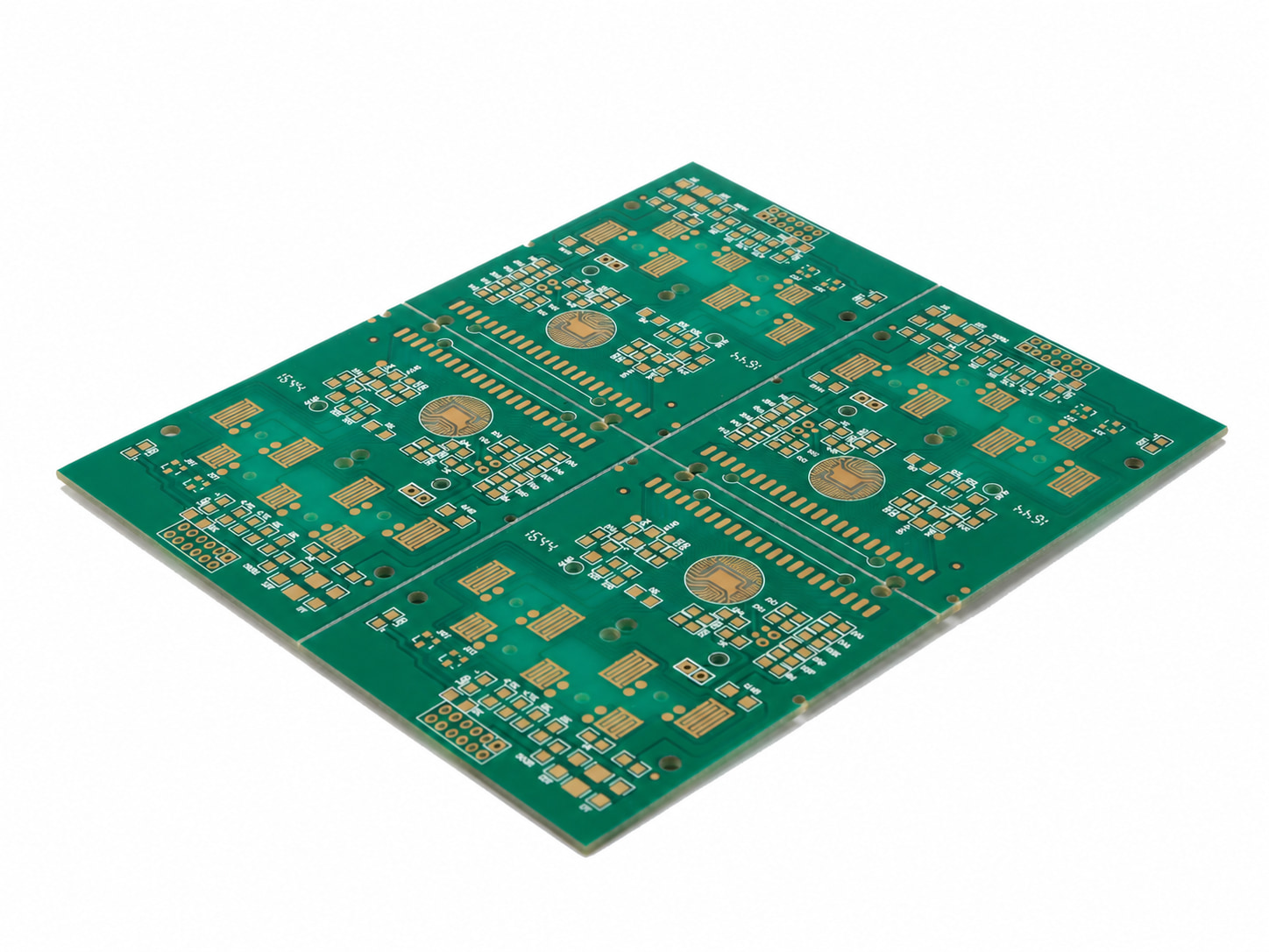
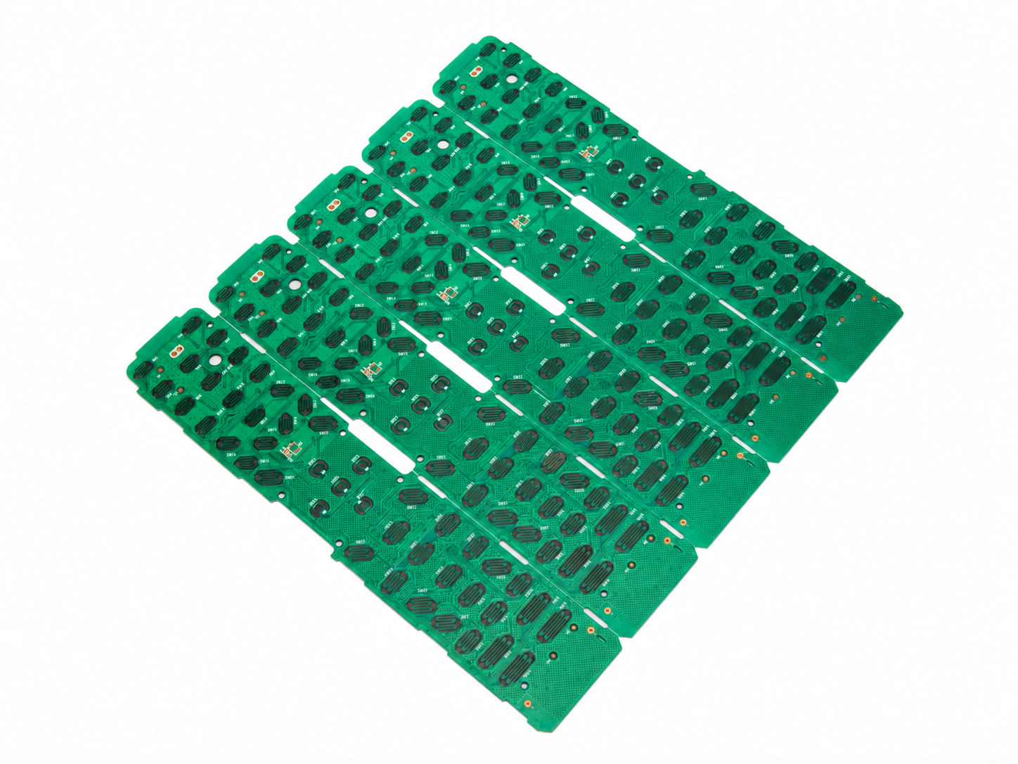
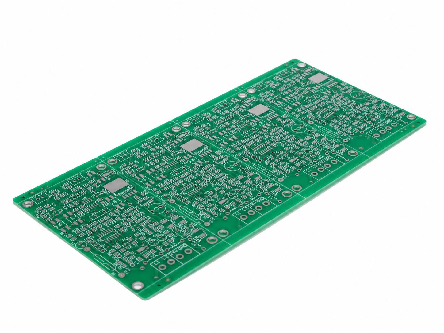
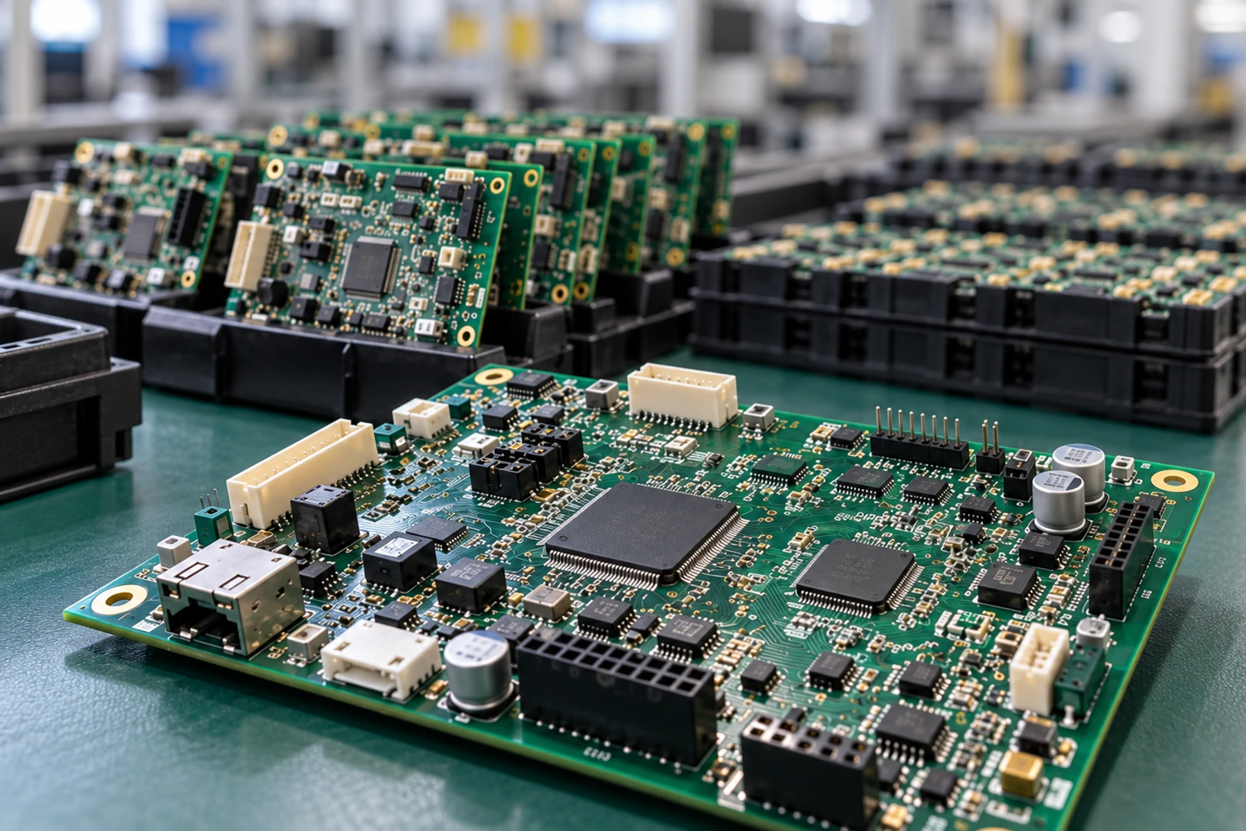
In global electronics manufacturing, the single-sided PCB (also known as single layer PCB) remains the ideal choice for balancing high-volume production with strict budget control. We specialize in delivering highly reliable, cost-effective single-sided printed circuit board fabrication and turnkey assembly services. By utilizing premium industry-grade substrates — including standard FR-4, economical paper-based FR-1/FR-2 and composite CEM series, and thermally conductive aluminum-based substrates — combined with precision processing equipment, we apply material selection and process controls to support reliable thermal, electrical, and mechanical performance for the agreed design requirements. From fast-turn consumer electronics and high-power LED lighting to stable automotive electronics, we adapt our manufacturing processes and quality control procedures to meet your specific cost and quality requirements, providing an optimal, scalable manufacturing solution for your project.
What is a Single-Sided PCB?

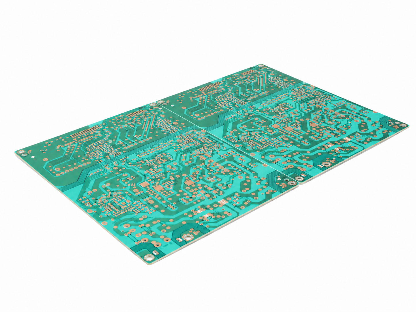
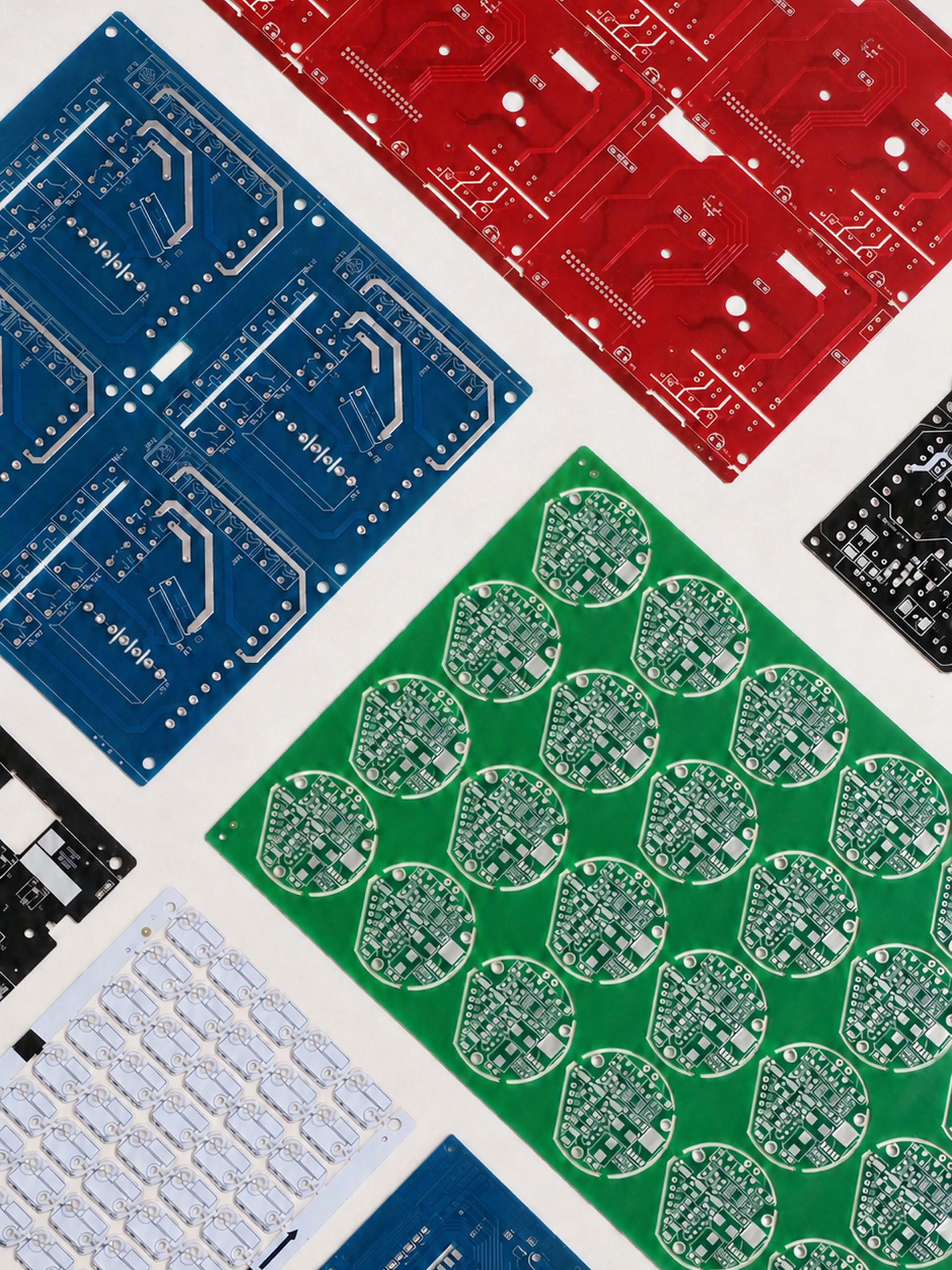
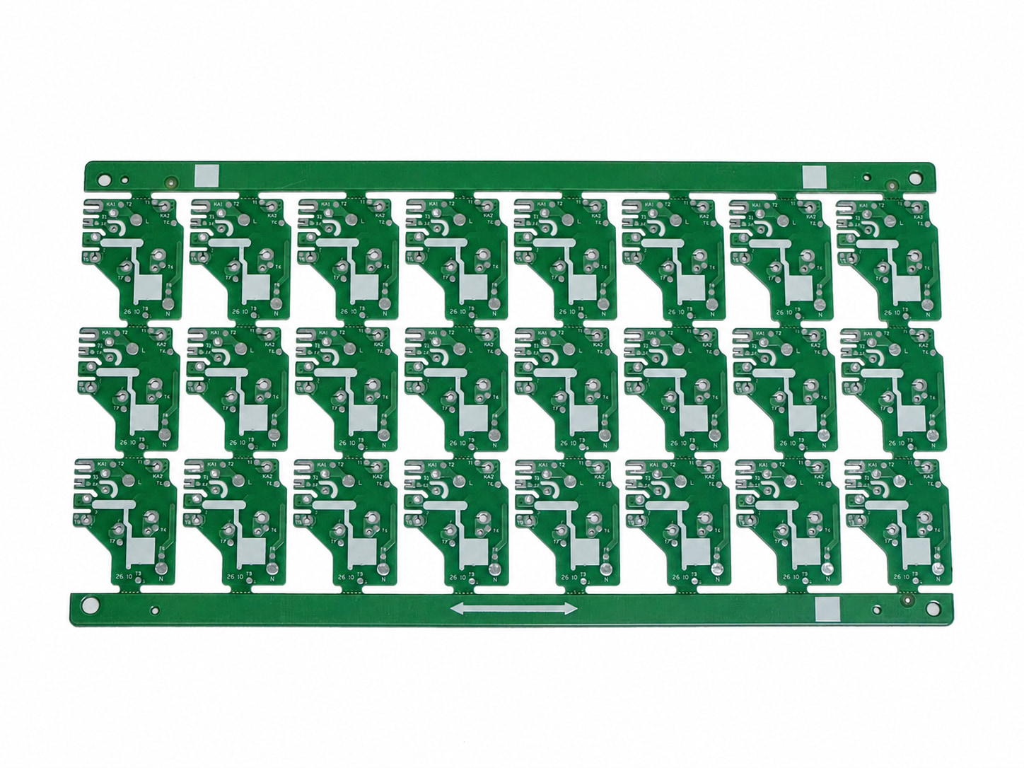
A single-sided PCB, also called a single layer PCB or single-sided circuit board, is a highly reliable and cost-effective choice for straightforward electronics, featuring a single layer of copper traces and a protective solder mask on one side of an insulating substrate. If your project demands high-volume production and strict cost control, this streamlined structure offers an efficient solution to minimize manufacturing expenses and shorten lead times. To align with your specific application requirements, these boards are commonly fabricated on dependable base materials like standard FR-4, economical paper-based and composite laminates (FR-1, FR-2, CEM-1, CEM-3), or heat-dissipating aluminum substrates.

Key Advantages Of Single-Sided PCBs

Outstanding Cost-Effectiveness

Perfect for high-volume production in price-sensitive industries like consumer electronics. The streamlined, single-layer structure minimizes raw material and processing expenses, helping reduce overall production costs and strengthening your cost competitiveness.

Design Simplicity & Efficient Turnaround

Compared with multilayer PCBs, single-sided boards typically require fewer fabrication stages. This simplified process supports efficient production scheduling for suitable projects and helps bring products to market sooner.

Structural Reliability with Fewer Failure Points

With only one conductive layer and no inter-layer connections, single-sided PCBs inherently have fewer potential failure points than multilayer designs. This translates to more stable, consistent manufacturing outcomes and lower defect rates for designs suited to a single conductive layer.

Versatile Substrates & Enhanced Thermal Management

Single-sided PCBs accommodate diverse substrate types — including FR-4, economical paper-based FR-1/FR-2 and CEM series, and thermally conductive aluminum-based substrates (MCPCB / Metal Core PCB) — to match varied application requirements. The aluminum-based option delivers improved heat dissipation for LED lighting and power electronics, with actual thermal performance subject to the overall system design.

When to Upgrade to Double-Sided PCB

While single-sided PCBs deliver superior cost efficiency for basic applications, as product requirements grow in complexity, single-sided designs may reach their technical limits. The following are key technical indicators suggesting a transition to a double-sided PCB may be appropriate for your project:

Routing Layout Bottlenecks (Overlapping Traces)

When circuit complexity increases to the point where traces inevitably intersect, a single conductive layer can no longer accommodate routing without causing short circuits. A double-sided structure resolves this by enabling independent top-and-bottom layer routing, with inter-layer connections made via plated through-hole vias.

High Component Density

If your design incorporates a high number of electronic components, a single-sided surface may provide insufficient physical space for component placement and solder pads. Double-sided PCBs allow components to be populated on both sides, significantly expanding the available component placement area.

Compact-Size Constraints

When the end product demands strict size constraints, a single-sided layout may struggle to accommodate all required circuitry within the available board area. A two-layer architecture provides additional routing and component-placement flexibility, potentially reducing board area for the same circuit function.

Signal Integrity & Power Distribution Requirements

For designs operating at higher frequencies or requiring tighter signal control, a single conductive layer lacks a dedicated reference plane, making it difficult to manage signal return current paths and control trace impedance. Double-sided PCBs provide greater flexibility in organizing ground and power networks, enabling improved return-path management and signal-integrity design when properly engineered.

When to Upgrade to Double-Sided PCB

Manufacturing Capabilities

Looking for detailed mechanical or electrical processing capabilities?

To optimize your browsing efficiency, we have consolidated our verified baseline capabilities into a single reference matrix. Access our master data sheet below to review complete technical parameters across all 1-8 layer PCB products.

Access Master Capabilities & Technical Specs →

Single-Sided PCB
DFM Guidelines

Get a Quote

Large Copper Area Optimization (Warpage & Etching Uniformity)

For single-sided designs, extensive solid copper pour areas can lead to board warpage during thermal processes due to unbalanced stress on a single conductive layer; they can also cause localized etchant saturation, resulting in uneven etch rates and edge over-etching. For large copper areas, copper balance, current-carrying capacity, thermal performance, and assembly requirements should all be reviewed before selecting cross-hatched or solid copper pours.

Copper Thickness Vs.
Trace/Space Allocation

Trace width and spacing must scale with copper weight. While our manufacturing limit reaches 4/4 mil on standard 1 oz copper, heavy copper boards require wider allocations — for 2 oz copper, design at ≥ 5/5 mil; for 3 oz copper, design at ≥ 8/8 mil. Thick copper requires wider spacing to prevent lateral over-etching or residual copper bridges; please refer to our manufacturing capability datasheet for the full matched guidelines.

Panelization For Small Form-
Factor Boards

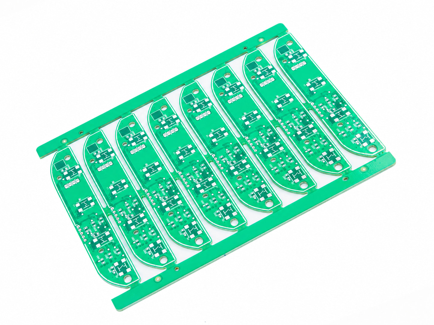
For individual boards below 70 × 70 mm, early panelization review is recommended. Panel delivery can improve handling, profiling and shipment of bare PCBs; when automated assembly is selected, it can also support printing, placement and line efficiency. The panel format, rails and breakaway method are confirmed against the outline, assembly route and downstream depaneling requirements.

V-Cut To Conductor
Clearance Safety Margins

To prevent copper exposure, lifting, or short circuits during the board de-panelization process, the clearance between the V-cut score line and any adjacent copper traces or pads must be maintained at ≥ 0.4mm.

The Sunhope Solution

Overcoming Single-Sided PCB Manufacturing Challenges

Challenge 1Warpage Control & Flatness Management
Warpage Control & Flatness Management

The Challenge

Single-sided PCBs are prone to warpage during thermal processes like HASL (Hot Air Solder Leveling) due to asymmetrical single-layer copper stress.

Sunhope's Solution

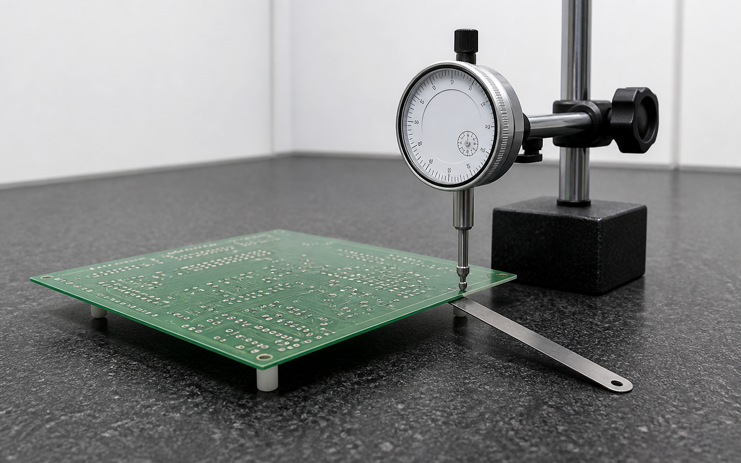
Warpage control begins with material construction, copper distribution, panel design and the relevant thermal route. For applicable boards, SUNHOPE uses thermal-equalization baking, controlled cooling and precision leveling or flatness verification to manage residual stress. Bow and twist are checked against the applicable IPC or customer-agreed criteria before delivery or subsequent assembly.

Micro-Crack & Burr Prevention in Die-Punching

The Challenge

Cost-effective materials (such as FR-1, FR-2 or CEM-1 paper-based and composite laminates) are brittle at room temperature and can easily develop micro-cracks or hole-edge burrs during high-speed mass production stamping.

Sunhope's Solution

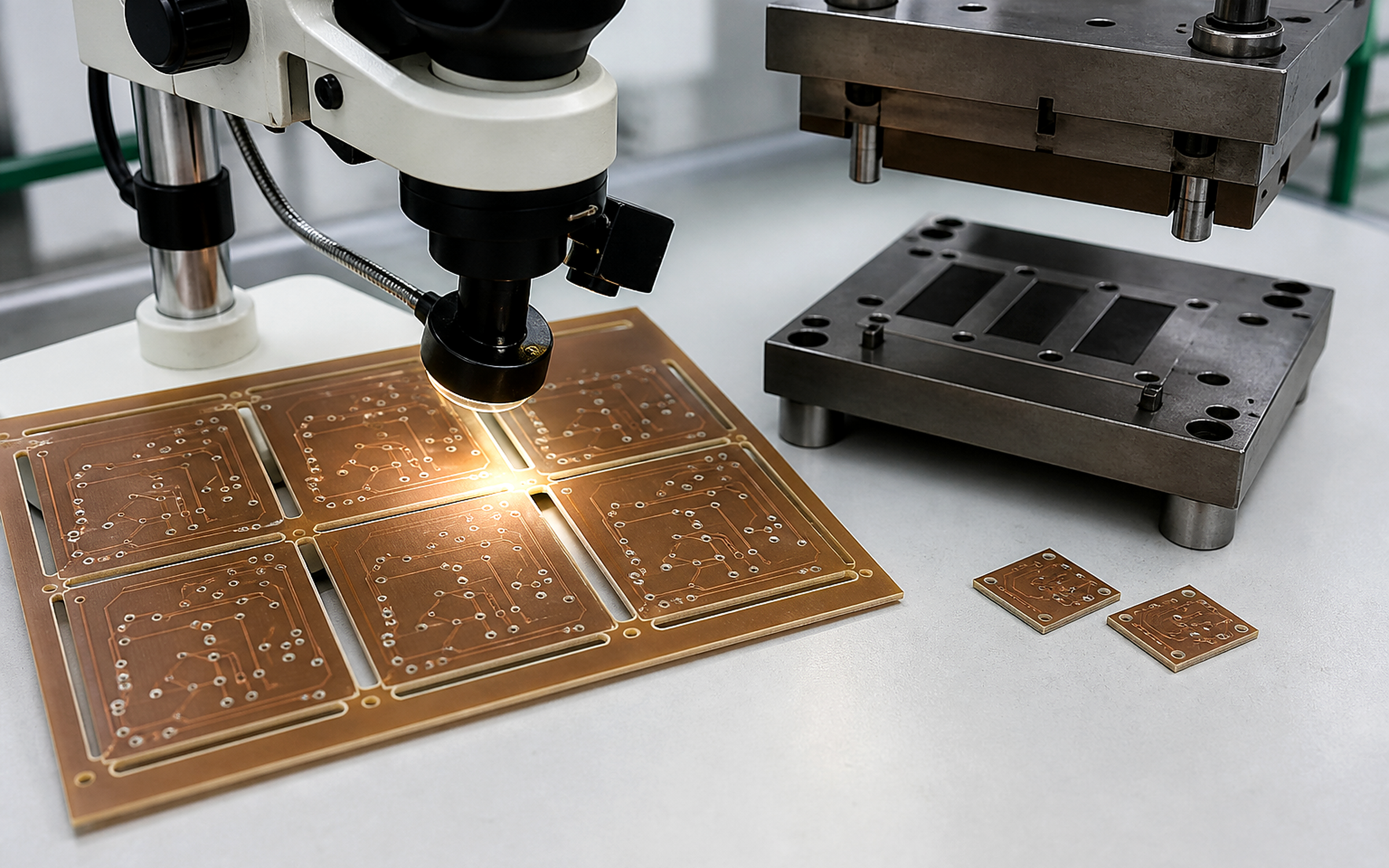
For single-sided projects utilizing die-punching, Sunhope implements a precision infrared localized pre-heating system to bring the substrate to its optimal softening point before stamping. Coupled with a strict, digitized tracking system for die wear life, these controls help reduce burr, cracking, and delamination risks during die-punching production.

High Pad Adhesion & Solder Mask Anti-Bleeding

The Challenge

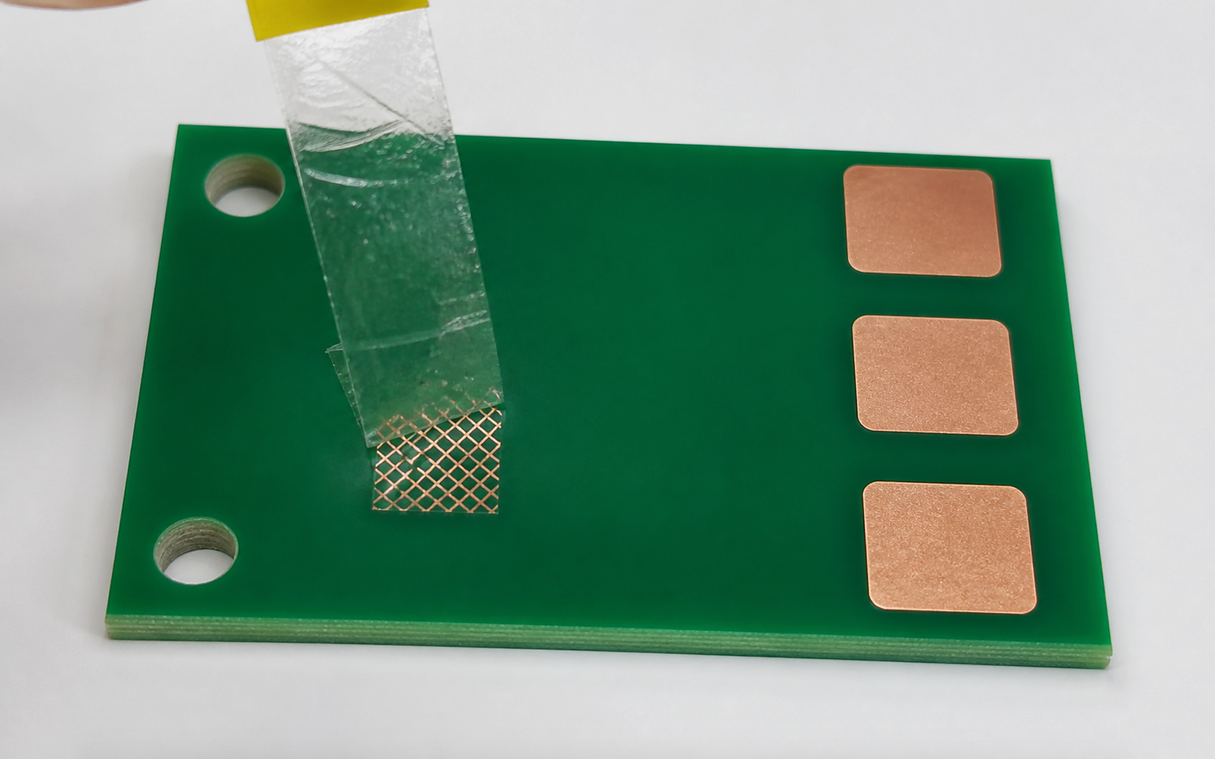
Single-sided PCB designs commonly use NPTH; where PTH is specified, the processing requirements are confirmed during engineering review. Pads rely purely on surface adhesion and can easily lift during soldering. Additionally, solder mask ink can easily bleed onto these pads during printing.

Sunhope's Solution

We control chemical micro-etch depth through the defined process and digital optical monitoring, promoting consistent copper-surface preparation and adhesion. High-viscosity solder-mask ink and tuned squeegee-pressure settings help control ink bleeding and mask encroachment, supporting clean pad definition and subsequent solderability.

Advanced Reliability for Aluminum LED PCBs

The Challenge

White solder mask for LED applications is prone to yellowing under high curing or reflow temperatures. Additionally, microscopic aluminum burrs generated during V-scoring can cause high-voltage breakdown shorts.

Sunhope's Solution

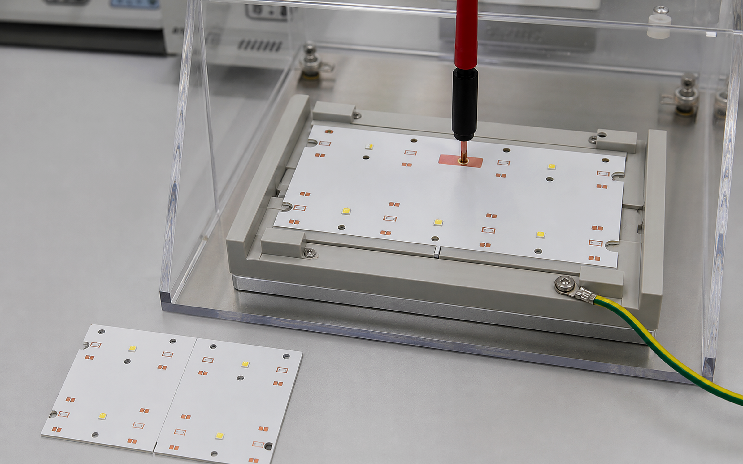
For LED and aluminum-core projects, SUNHOPE selects high-temperature, non-yellowing white solder mask and develops the curing profile around the approved material and soldering route, supporting reflectivity retention through the specified thermal exposure. V-scored edges are deburred where required, and Hi-Pot testing is available under agreed voltage, fixture, duration and acceptance criteria to verify the specified board-level insulation requirement.

Quality Testing & Inspection

Quality Testing & Inspection

To ensure every single-sided PCB delivered to you exhibits reliable, consistent performance and meets your cost and quality requirements, our facility implements a fully integrated digital quality control system. Our rigorous inspection and testing procedures include:

Electrical Testing (Available Upon Request)

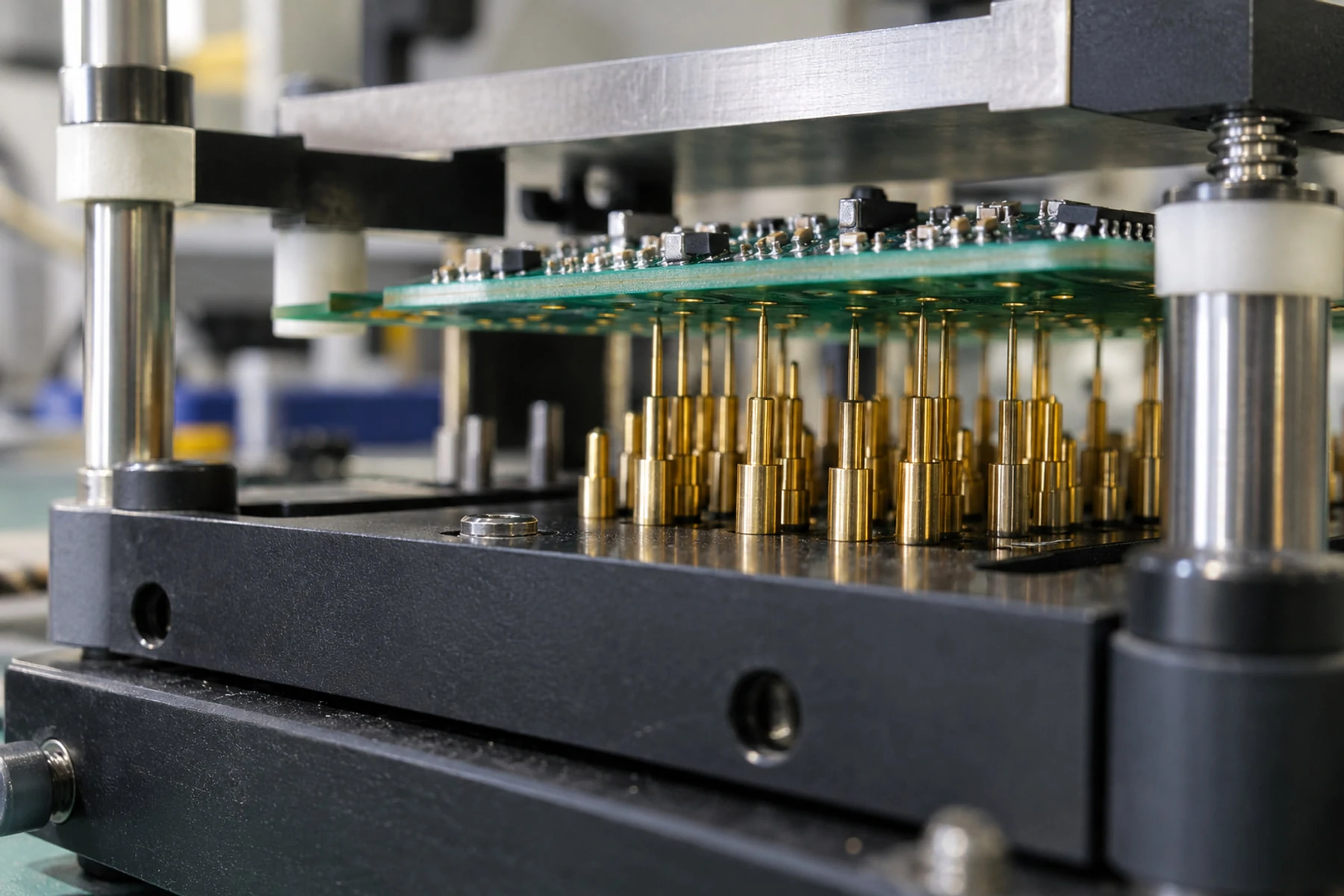
Depending on project volume and test requirements, 100% flying-probe testing or dedicated fixture testing can be arranged to identify opens and shorts before shipment.

High-Precision Circuit & Solder-Mask Inspection

AOI and targeted visual review are used at the applicable image and release stages to identify visible conditions such as opens, shorts, residual copper, pad contamination or solder-mask misregistration before shipment. This optical control complements—rather than replaces—the electrical test route defined for the order.

Dimensional & Mechanical Inspection

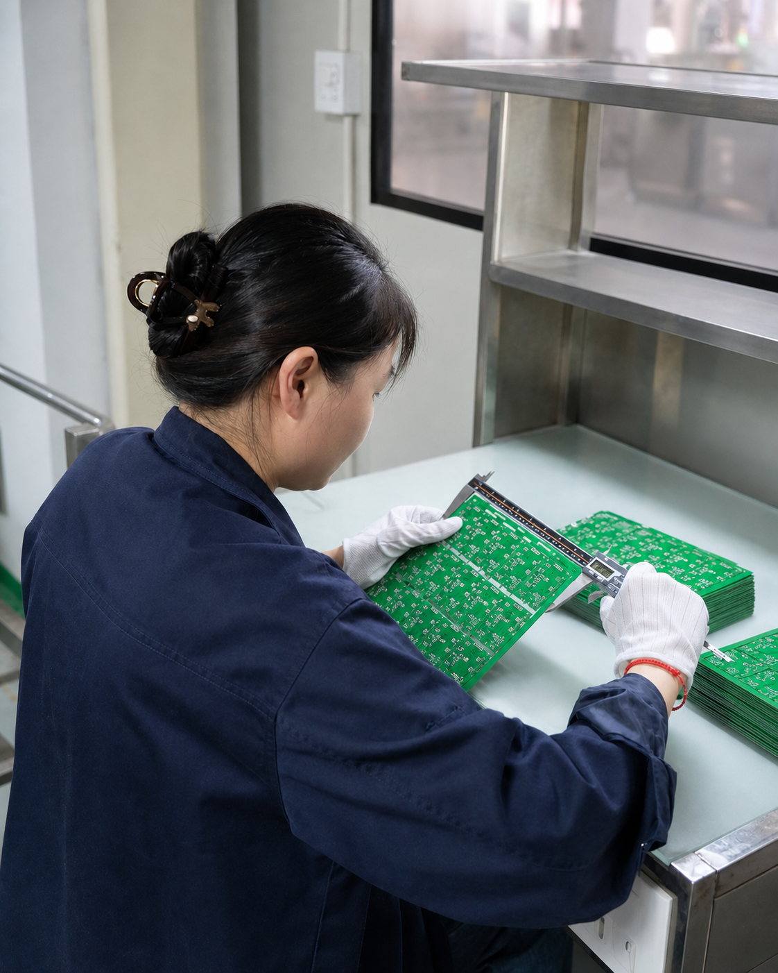
To ensure an accurate fit into your product housing, we strictly verify all board dimensions, board thickness, board outline and routing profiles, and V-cut depths against your technical drawings.

Surface Finish Quality Control

Rigorous inspection of the surface finish layer (such as OSP or HASL) to verify uniform coating thickness, excellent oxidation resistance, and storage life within specification.

Comprehensive Reliability Testing

Solderability Testing: To verify solder wetting performance and joint formation during your subsequent component assembly.
Thermal Stress Testing: To verify the substrate and copper foil's resistance against delamination and warpage when subjected to high-temperature lead-free reflow cycles.

Note: For advanced inspection requirements (such as cross-section analysis, accelerated aging tests, etc.), please contact our technical team directly. We are fully equipped to support your customized engineering specifications.

Certifications &
Compliance

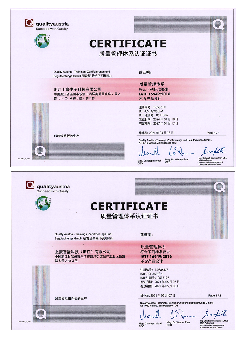
  • • IATF16949
  • • UL Certificate
  • • RoHS Compliance
  • • REACH Compliance
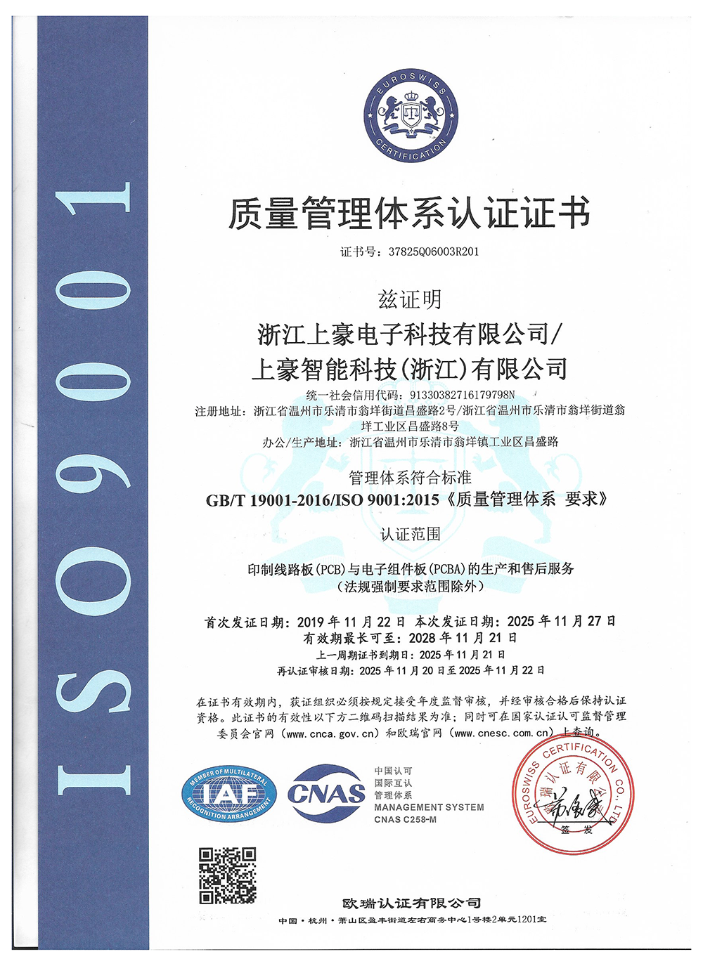
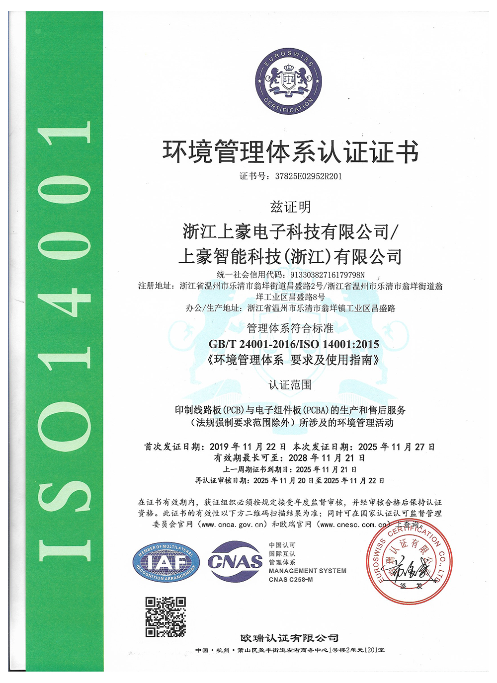
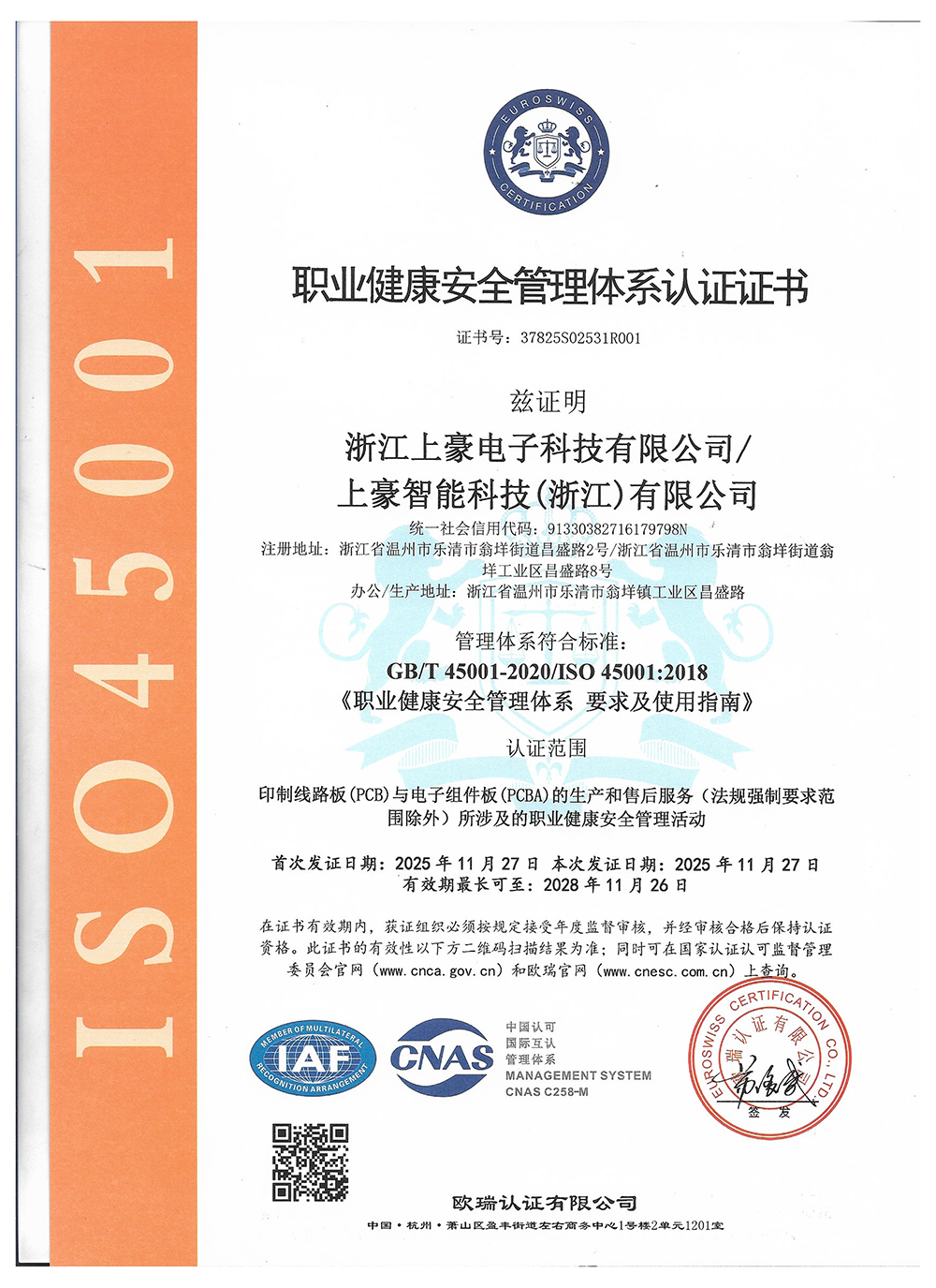
  • • ISO9001 / ISO14001 / ISO45001
More Certifications & Awards
IATF16949
IATF16949
ISO9001
ISO9001
ISO14001
ISO14001
ISO45001
ISO45001

Target Applications of Single-Sided PCBs

LED Lighting & Displays

Widely utilized in high-power LED bulbs, commercial tube lights, outdoor street lighting PCB modules, and various indoor/outdoor backlight display modules (Well-suited for Aluminum substrate / MCPCB applications).

Product FAQ

Have more questions? 
Visit our Comprehensive FAQ Center for more detailed information.

View More FAQ
What is the core difference between a single-sided aluminum-core PCB and a standard single-sided FR-4 PCB?

The primary difference is the board-level heat path. Common aluminum-core material grades publish dielectric thermal conductivity around 1–3 W/m·K, compared with roughly 0.3 W/m·K for standard FR-4—typically about 3–10 times higher depending on the selected grade and test method. This makes aluminum-core construction attractive for suitable LED lighting and power modules. Overall thermal performance still depends on dielectric thickness, copper distribution, interfaces, enclosure and system cooling.

The most common reasons for single-sided boards being flagged are the inclusion of Plated Through-Holes (PTH) or castellated edges (half-holes), which standard single-sided processes typically do not support. If your layout requires these configurations, or if there is a conflict between your line width and copper weight, our engineering team will reach out as soon as possible to offer professional engineering recommendations.

Coverage is defined by design complexity, production stage and acceptance requirements. We recommend 100% flying-probe or fixture testing for prototypes, new part numbers and risk-sensitive applications. Mature, low-complexity volume designs may use a quotation-approved, cost-optimized inspection plan, while agreed visual, dimensional and process controls remain in place. Optical inspection does not replace continuity and isolation testing.

Equipped with high-precision CNC drilling and specialized mechanical routing/V-scoring machinery, we fully support standard profiling, V-scoring, and precise non-plated cutout operations on aluminum boards. Since metal substrates impose unique mechanical tolerances, please include your specific technical descriptions for any complex slotting, irregular shapes, or heavy-gauge aluminum substrate designs so our team can evaluate them accurately.

OSP (Organic Solderability Preservatives) creates an exceptionally flat pad surface (whereas HASL can leave micro-convexities on pads), making it highly beneficial for fine-pitch SMT assembly, alongside an excellent cost advantage. However, if your boards require long-term storage (e.g., over 6 months) or must undergo multiple reflow passes, Lead-Free HASL or ENIG will provide superior long-term oxidation resistance and soldering durability.

Their asymmetric copper and material construction can create uneven stress during thermal processing. SUNHOPE reviews copper balance, material construction, profiling and the thermal route, then applies pre-bake, controlled cooling or additional leveling where the material and process require it. Finished boards are verified against the applicable IPC or customer-agreed flatness criteria.