Factory Tour & Process

Precision Manufacturing: Inside Our PCB & PCBA Factory

Where Engineering Meets Execution

Where Engineering MeetsExecution

15,000 m² of Visible Manufacturing
from Engineering Review to Final Shipment.

When you partner with Sunhope, your design does not disappear into a manufacturing “black box.” It moves through a visible sequence of engineering review, material preparation, PCB fabrication, assembly, inspection and shipment—supported by the people, equipment and process controls shown on this page. Our principle is simple: build quality into the process, not just inspect it at the end.

From 1–8 layer PCB fabrication to SMT, THT/DIP and mixed assembly, each project follows a manufacturing route shaped by its materials, construction and end-use requirements. Continue below to see the representative equipment and core process stages that turn engineering data into finished boards—and the checkpoints that keep that journey under control.

The Source Behind Every Board:
More Than Three Decades of Manufacturing Experience

Behind every reliable electronic product is a manufacturing system capable of turning design intent into repeatable production. Founded in 1993, Sunhope has spent more than three decades strengthening its expertise in PCB fabrication and PCBA assembly.

Today, our 15,000 m² manufacturing base and a team of more than 300 professionals support projects from NPI prototyping and pilot builds to volume production. With an annual PCB production capacity of 500,000 m², Sunhope brings together experienced people, established processes and practical manufacturing resources to help customers move from design data to finished products with greater clarity and confidence.

Dimension 1

Manufacturing Technology in Action

Where PCB & PCBA Manufacturing Capability Comes to Life

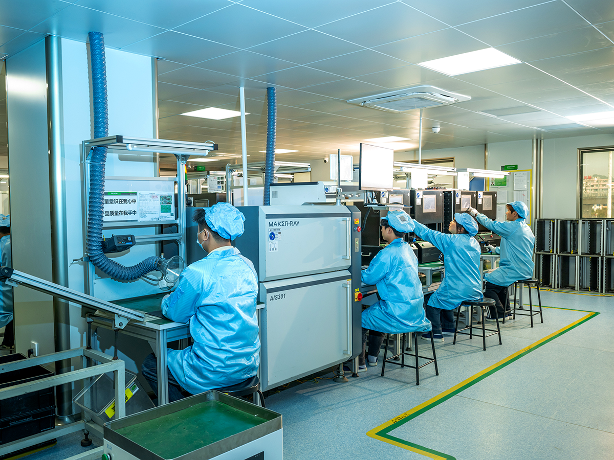
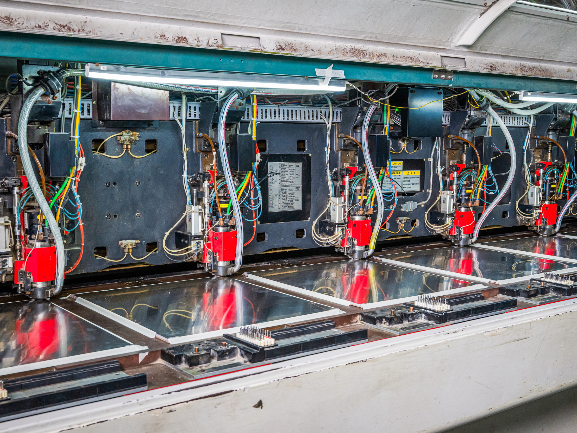
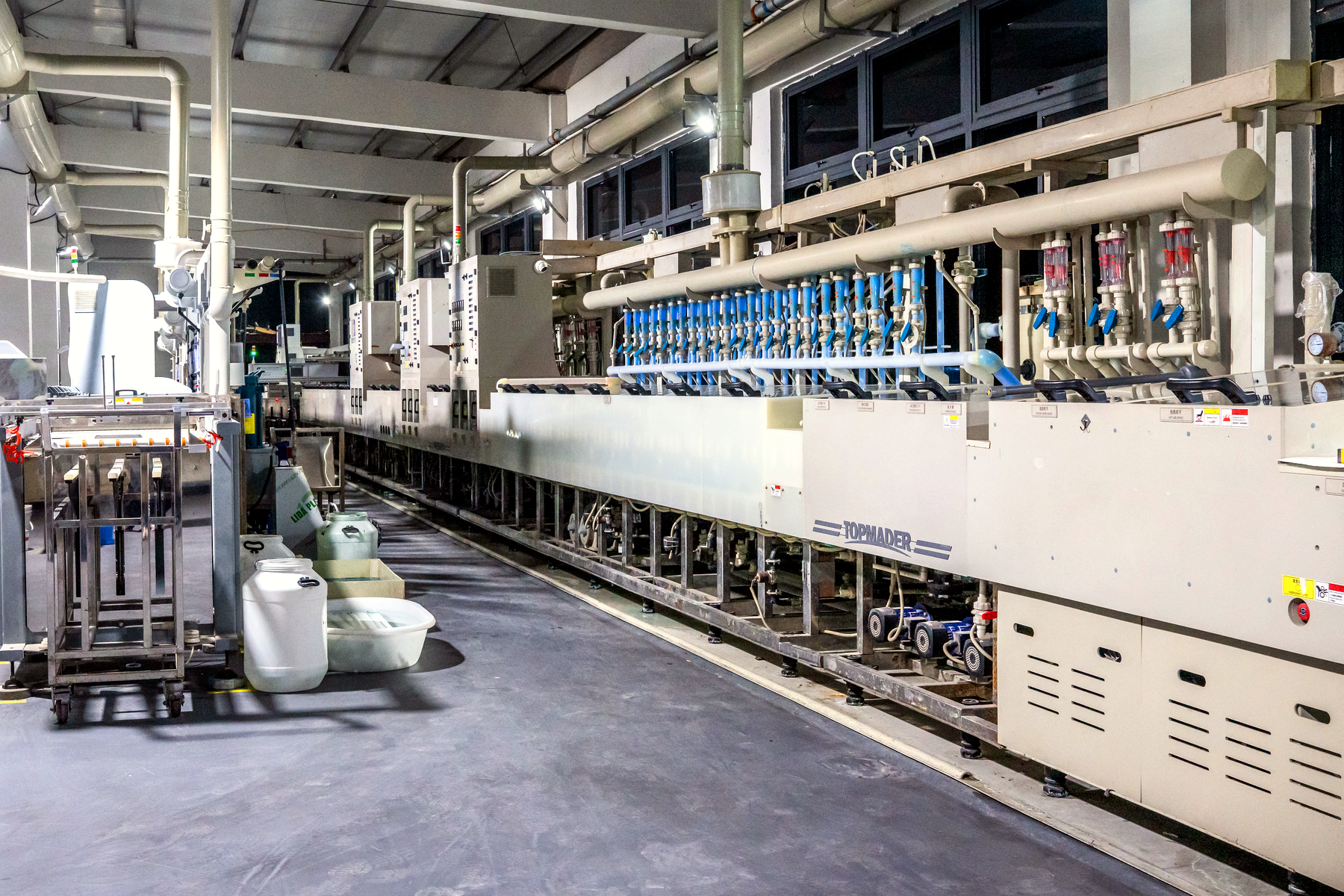
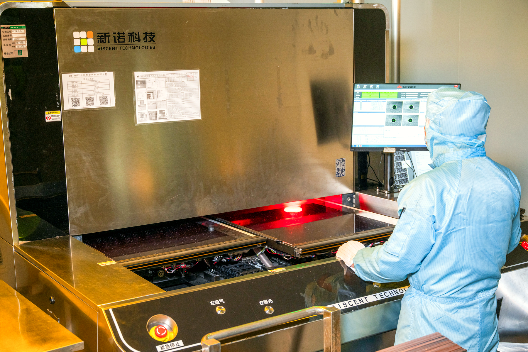
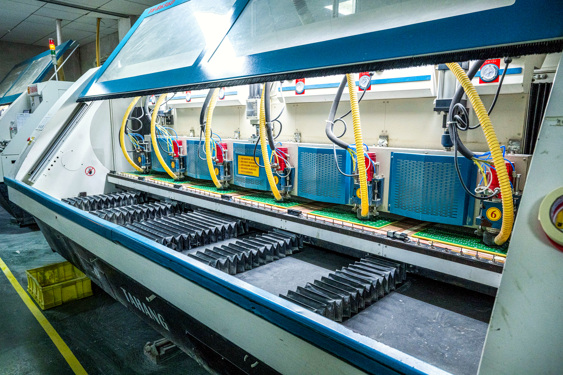
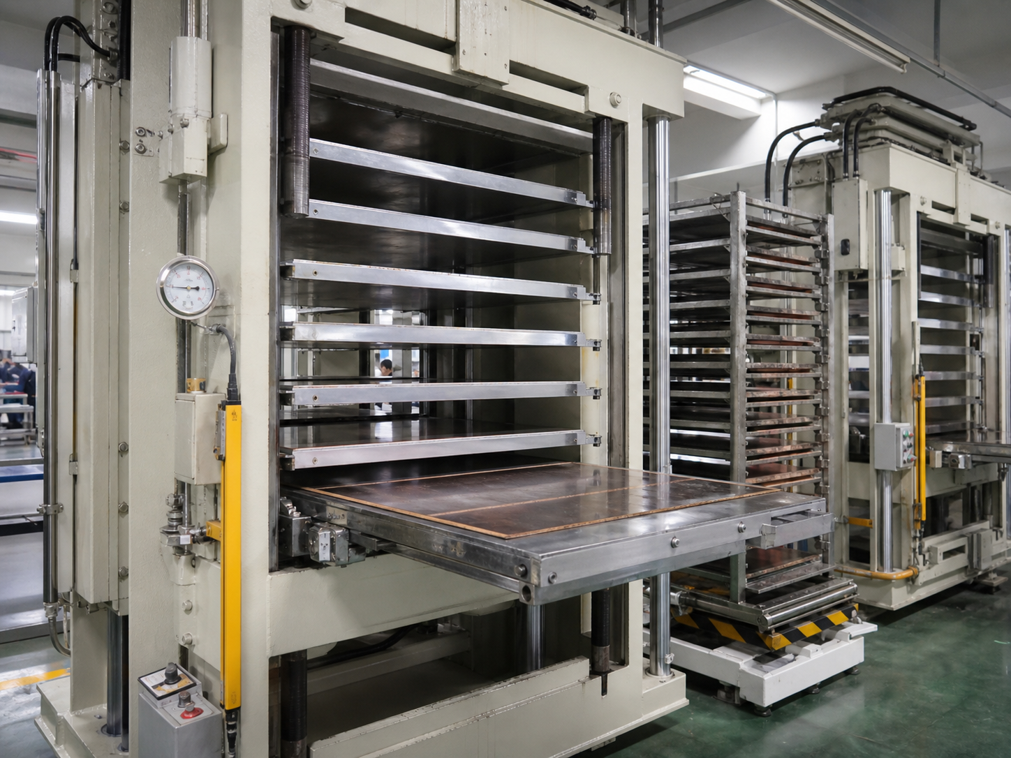
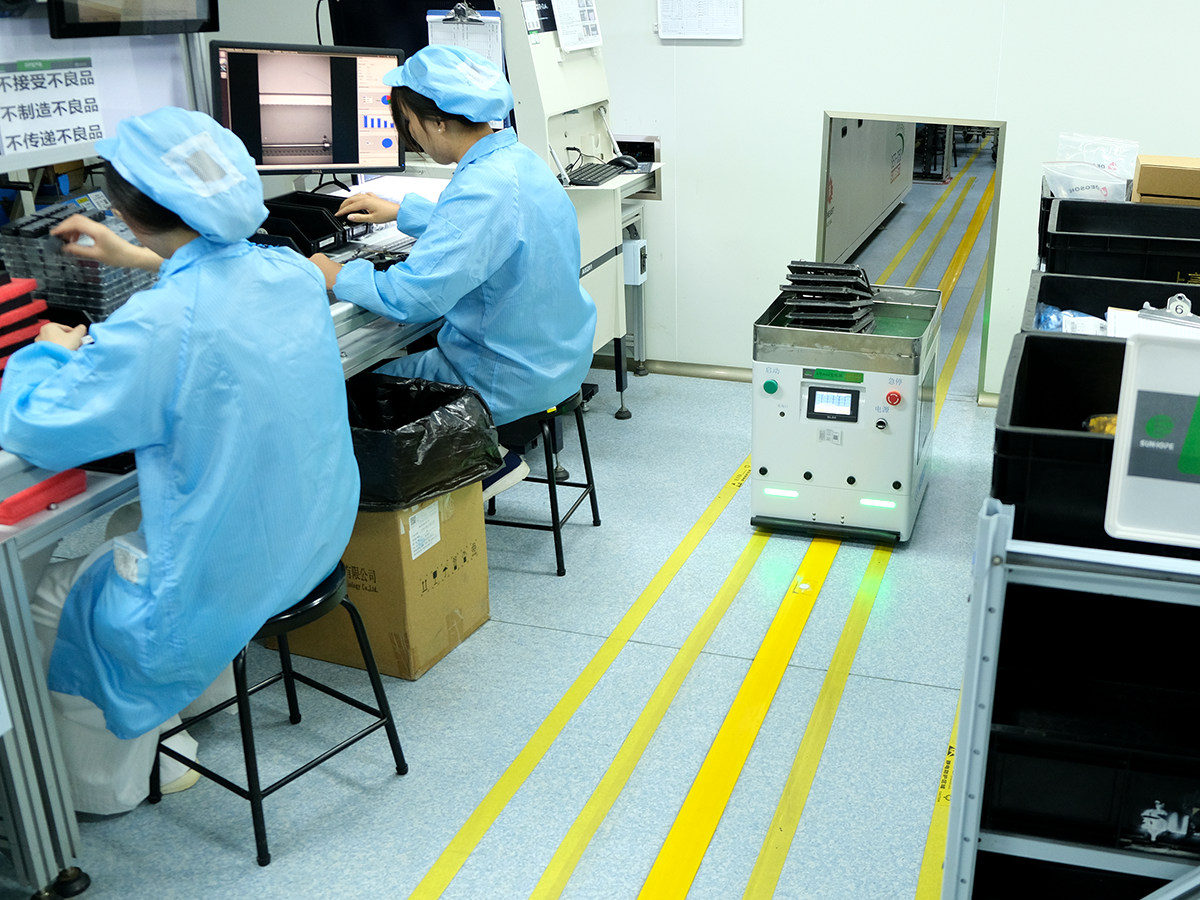
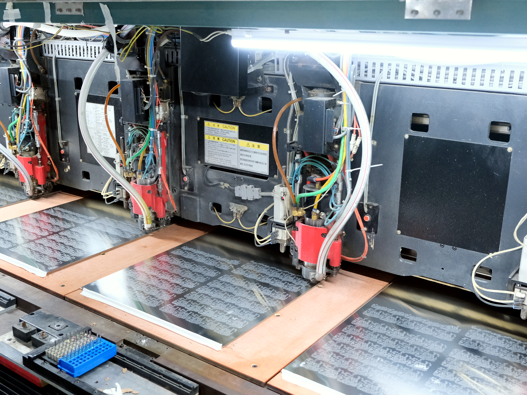
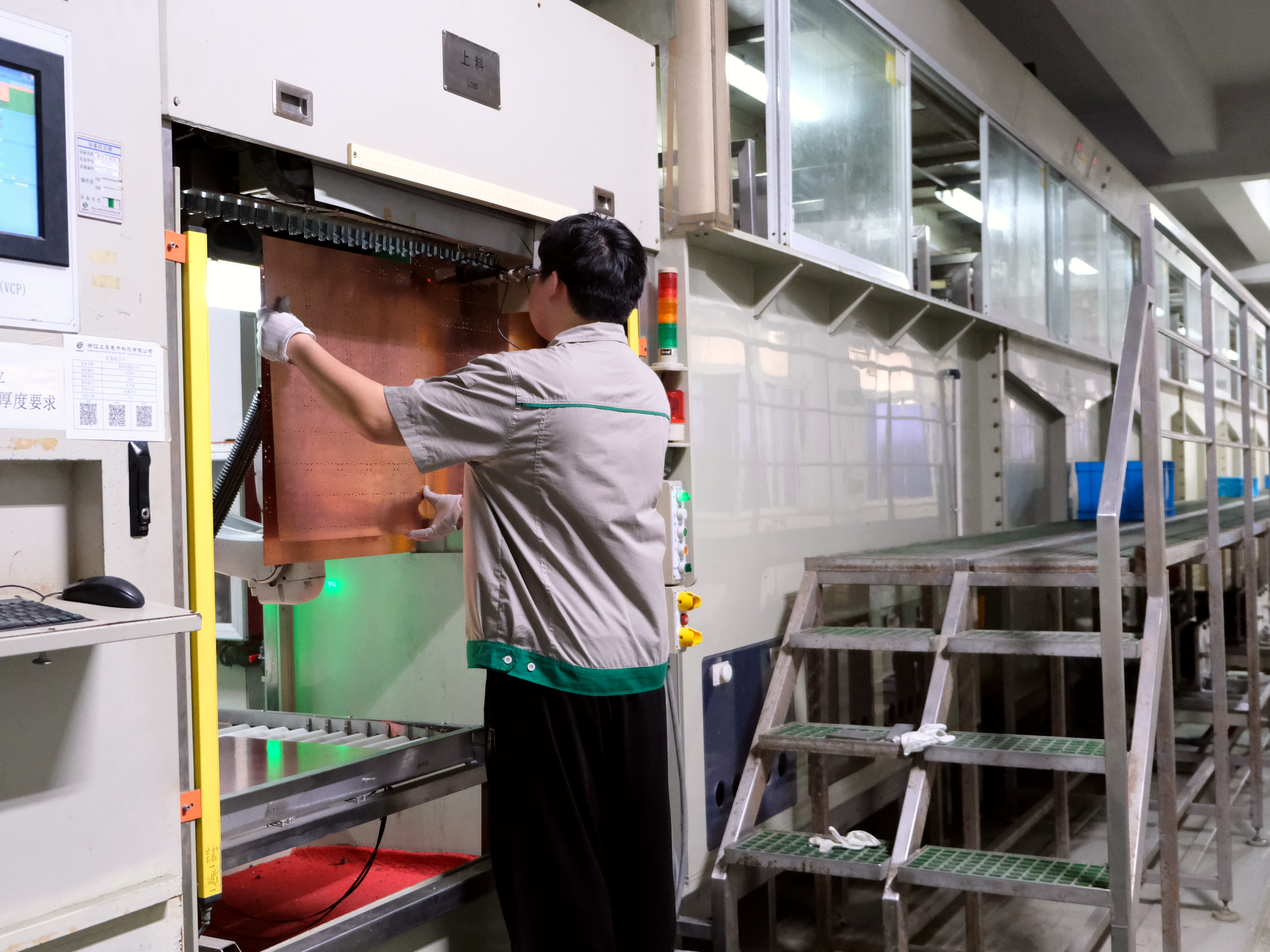
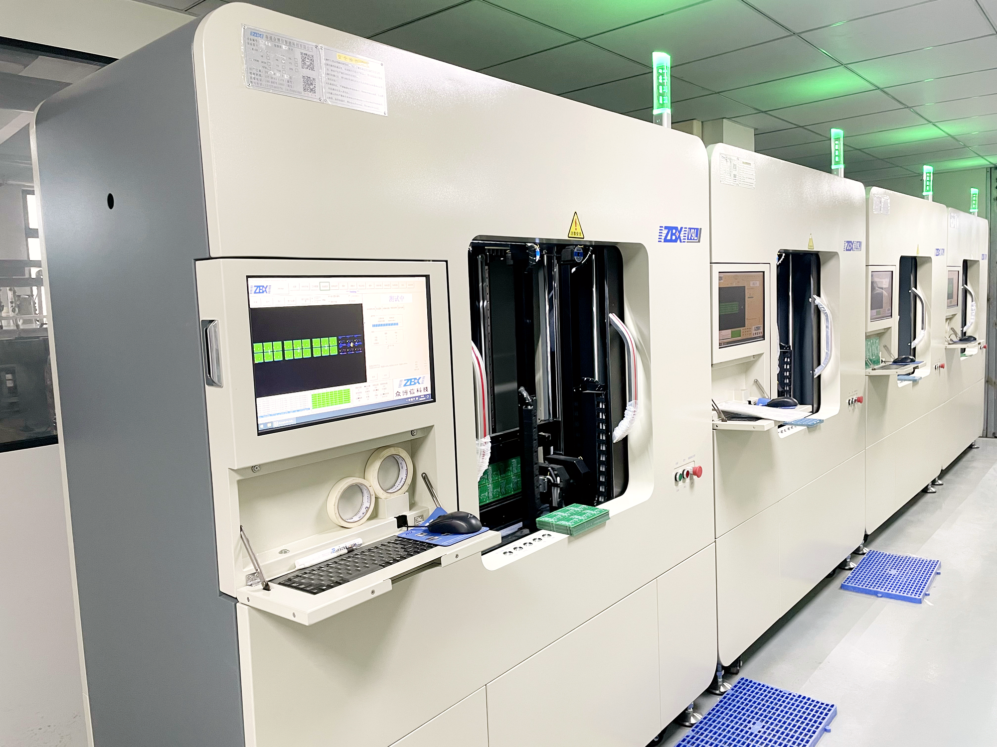
A capable factory is defined not by a list of machines, but by how effectively people, equipment and process control work together to turn engineering data into repeatable production. Across PCB fabrication and PCBA assembly, Sunhope connects these elements to support projects from NPI builds and pilot runs to volume production.

Manufacturing Technology in Action

Dimension 2

In-Process Inspection & Verification

Quality Philosophy: Build Quality into the Process, Not Just Inspect It at the End

Quality is strongest when it is protected at the stage where variation first appears. Sunhope connects engineering review, first-article confirmation, in-process inspection and final verification, allowing potential issues to be identified before they travel farther through production.

The exact inspection route is matched to board construction, assembly type, customer requirements and the approved control plan—so every checkpoint serves a clear purpose, rather than simply adding another box to tick.

In-Process Inspection & Verification
The Right Check, at the Right Stage

The Right Check, at the Right Stage

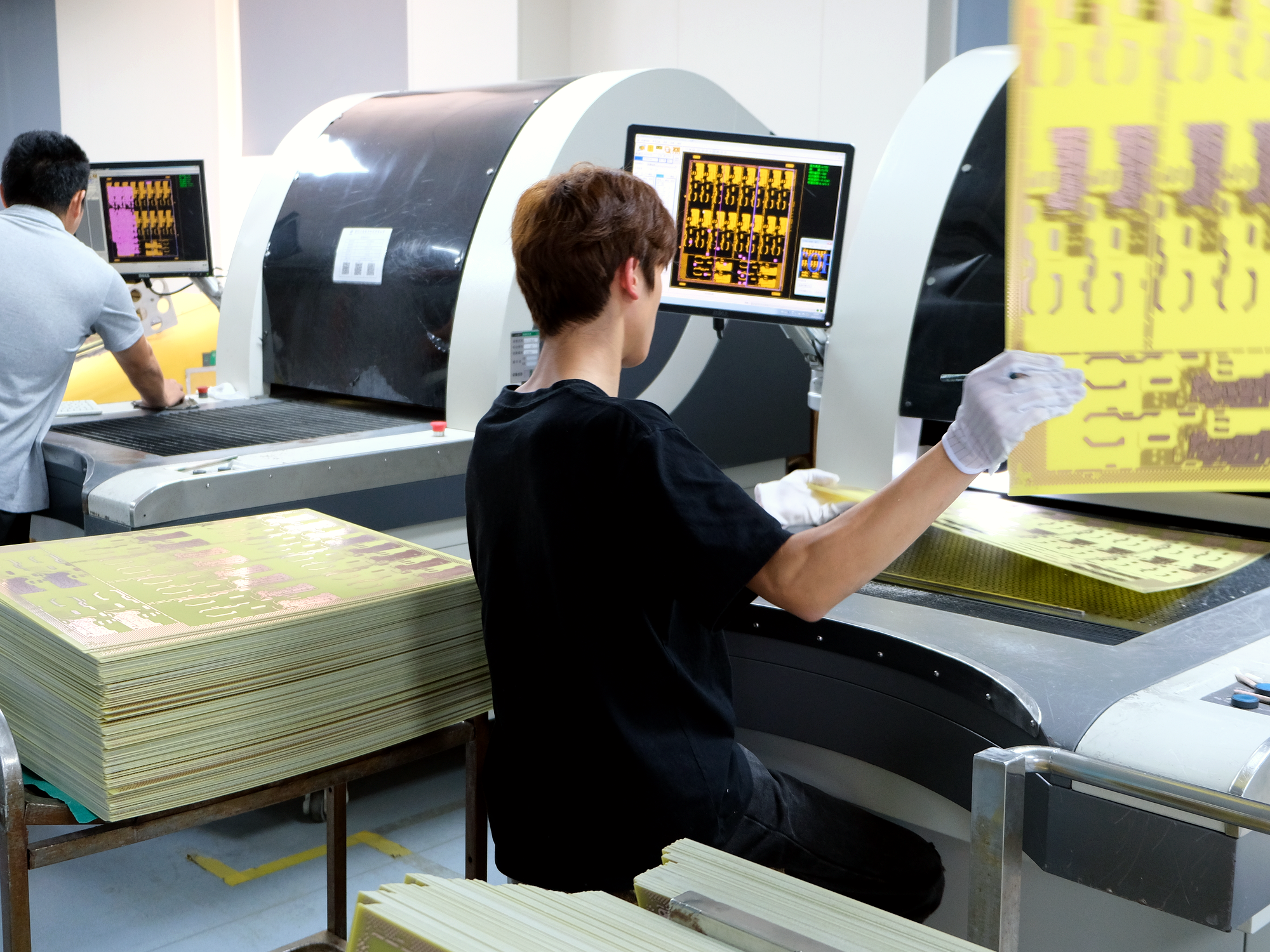
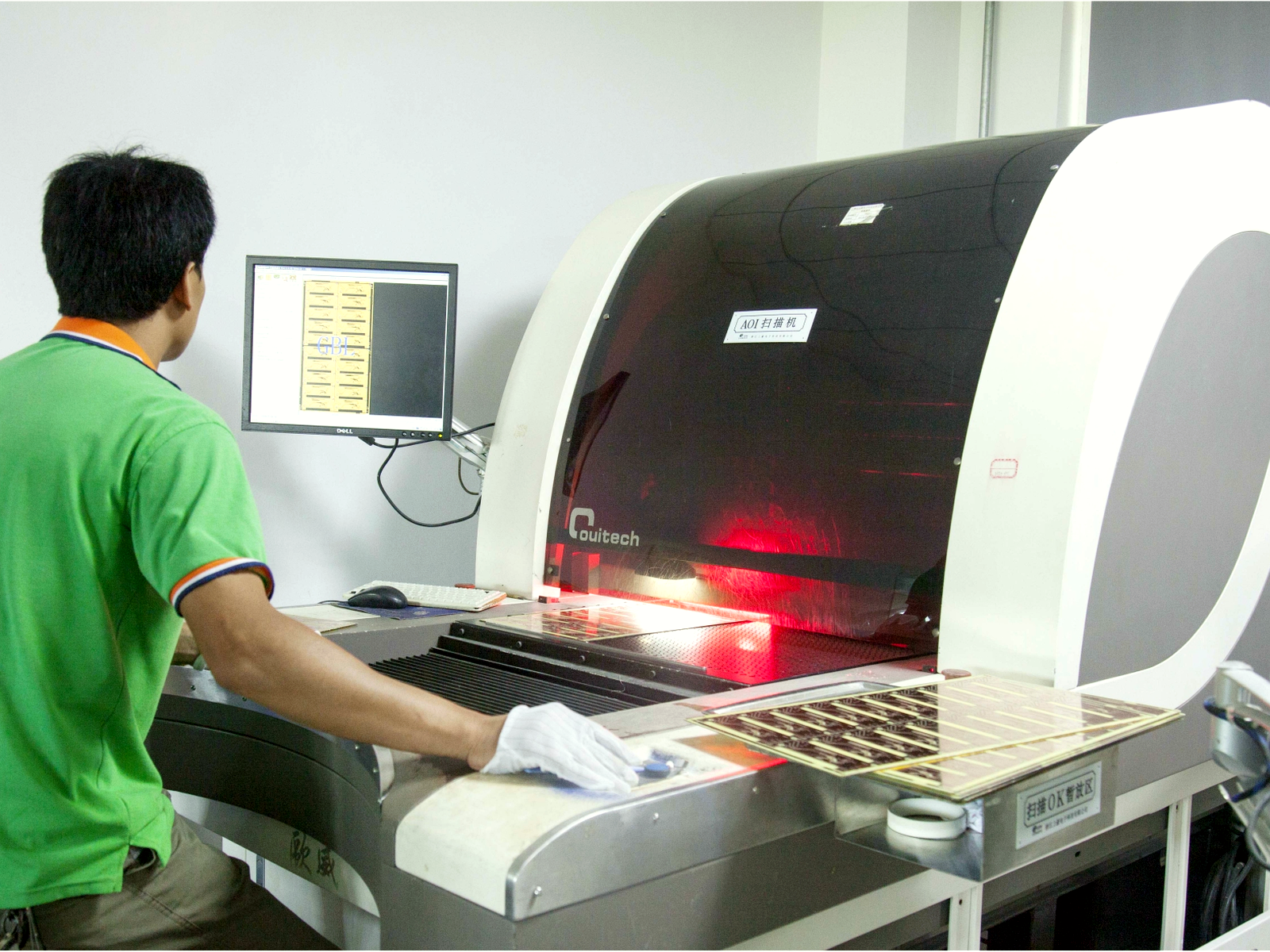
  • For bare PCBs: Quality control begins with engineering-data and material review before production, then follows the board through critical stages such as inner-layer imaging, lamination registration, drilling and plating, surface finishing, dimensional inspection and electrical testing. AOI and netlist-based electrical testing are applied according to board construction and the approved inspection route, helping identify pattern, registration, open/short and dimensional issues before shipment.
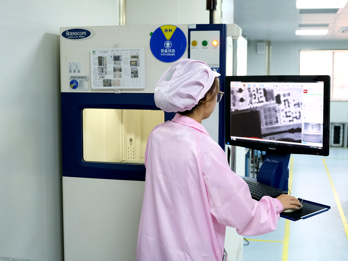
  • For PCB assemblies:Verification begins with component and line-setup checks, then follows solder-paste printing, component placement, reflow, THT soldering and final product testing as required. First-article inspection, SPI, AOI and X-Ray are applied where appropriate to the assembly design and control plan, while ICT or functional testing is performed when fixtures, programs and acceptance criteria have been agreed.
  • Detailed inspection capabilities, acceptance criteria and packaging controls are presented in our Quality Assurance & Packaging overview.

Dimension 3

Manufacturing Discipline & Traceability

A Controlled Environment. A Traceable Production Path

Reliable electronics are not manufactured in chaos. They take shape in a disciplined environment where materials, work areas, handling practices and production records are managed with purpose. At Sunhope, this discipline connects the physical factory floor with the information needed to understand how each production lot moves through manufacturing.

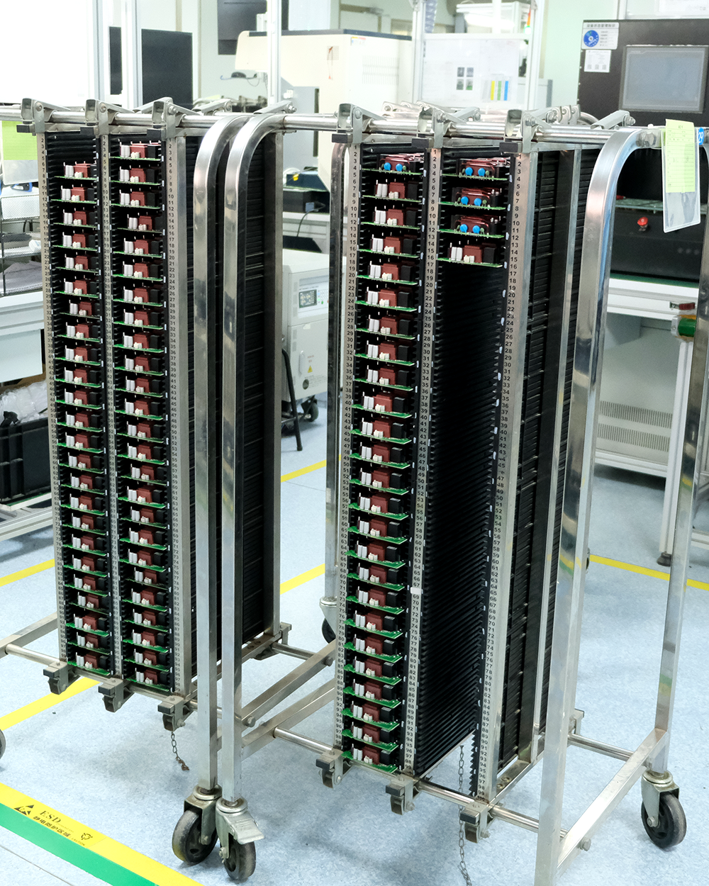
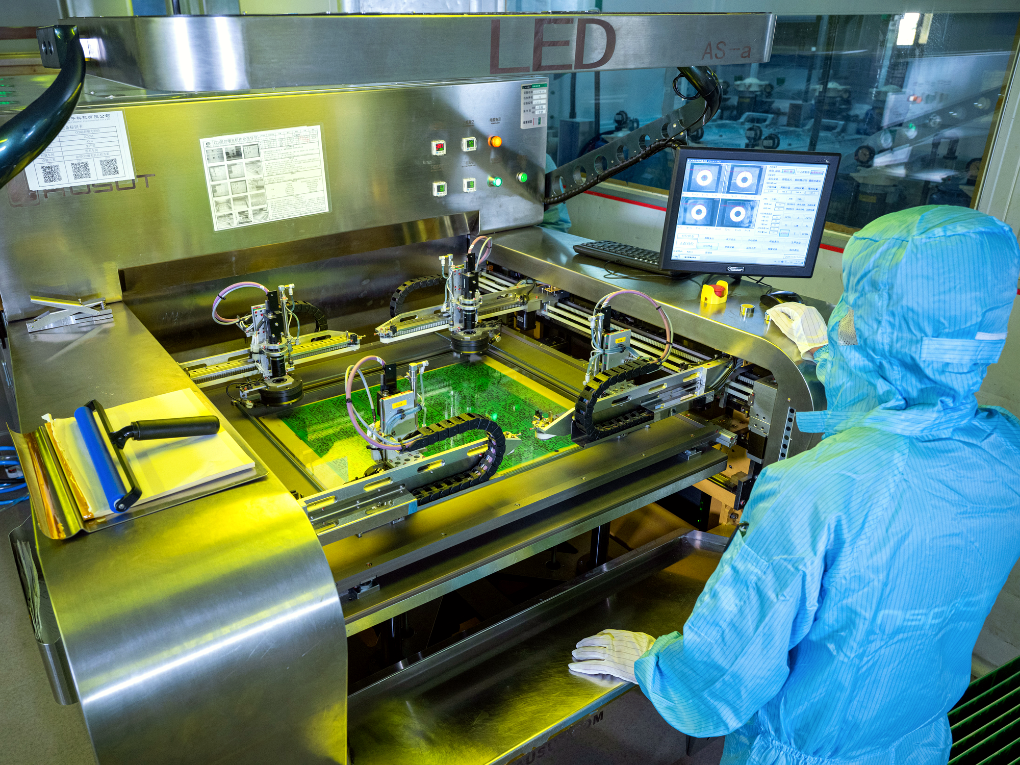
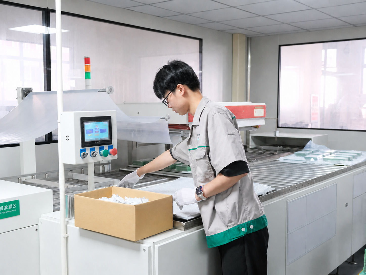
Process-sensitive areas are managed through defined housekeeping, material-handling, temperature and humidity controls, while ESD protection is applied across PCBA assembly operations. Together, these measures help protect photo-sensitive materials, solder paste, components and work-in-process products at the stages where environmental conditions matter most. Batch-level records connect incoming materials, production lots and completed PCBs or assemblies, supporting faster investigation, clearer customer communication and continuous improvement when questions arise. Where project and design conditions permit, laser-marked QR codes can add unit-level identification to PCB products. The exact traceability fields follow project requirements and the production records available for the order.

Manufacturing Discipline & Traceability

Process Demonstration
From Engineering Data to Finished PCB: 10 Core Manufacturing Stages

The sequence below follows a representative multilayer PCB route and uses ten core stages to show how engineering data, materials and process controls come together on the factory floor. Single-sided and double-sided boards follow shorter routes, while controlled impedance, high-Tg and high-frequency PCBs require additional material-and design-specific controls at selected stages.

Phase 1 Engineering Review & Material Preparation
Engineering Review & Material Preparation

Process

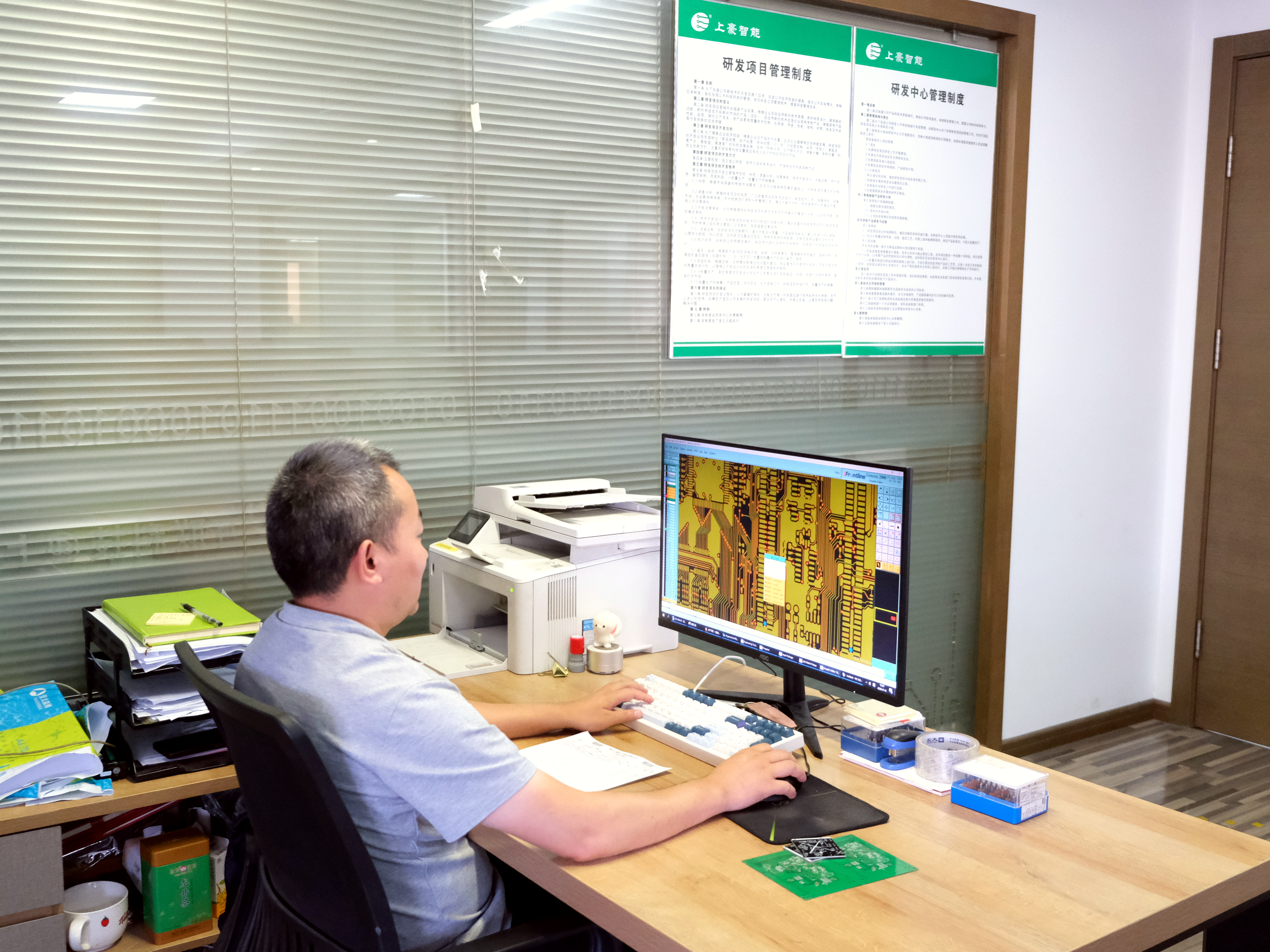
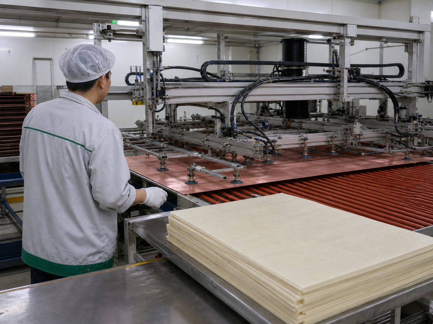
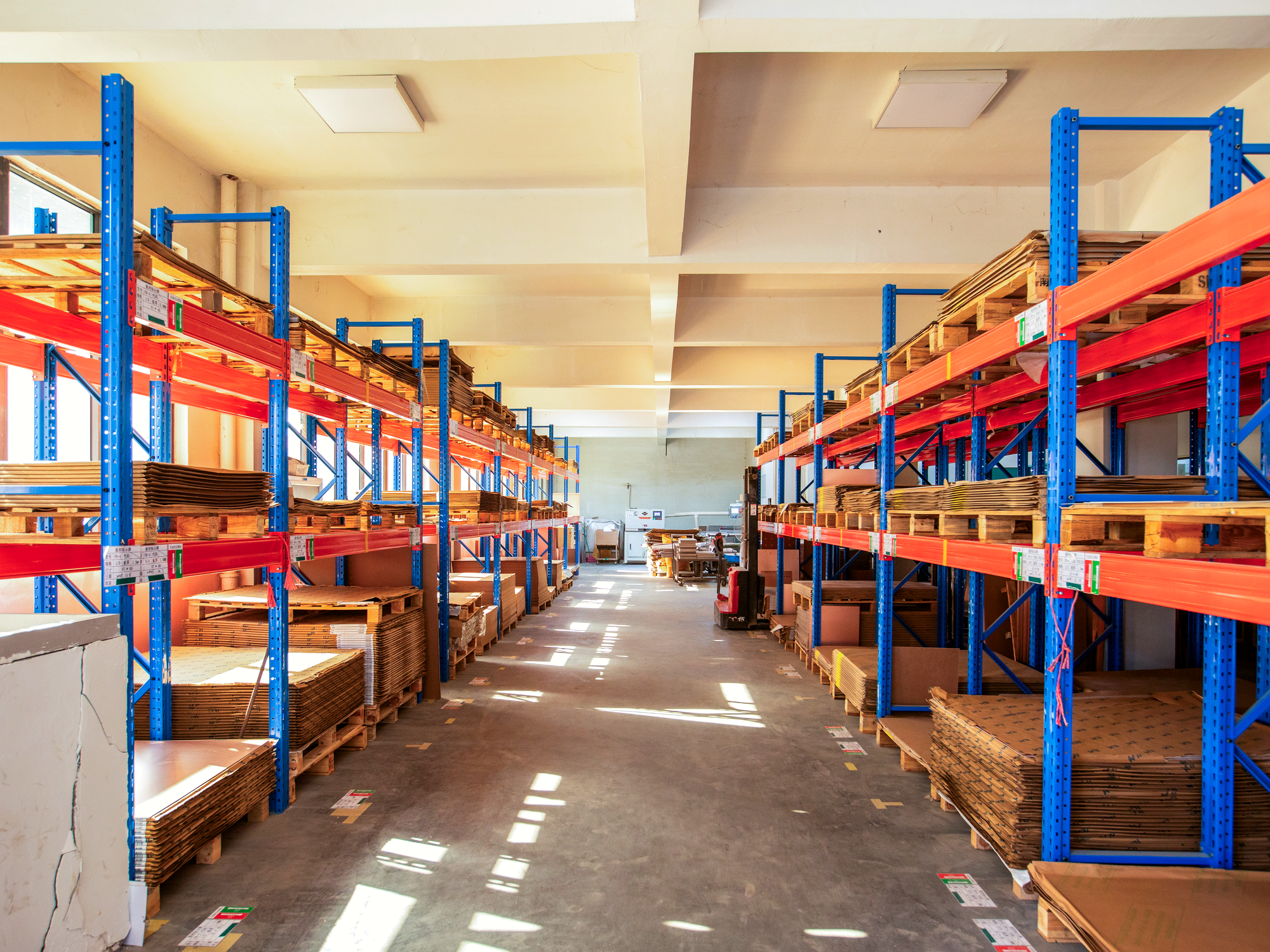
Customer fabrication data, drawings and order requirements are reviewed and translated into controlled CAM, panelization and manufacturing information. Materials are then issued and prepared against the approved board construction, copper weight, finished thickness, surface finish and acceptance requirements.

Key Control Points

File completeness and revision; board outline and layer sequence; material type, manufacturer and lot; copper weight and finished thickness; drill and routing data; surface finish; impedance targets, tolerances and test-coupon requirements where specified. For high-Tg and high-frequency products, verify the specified resin or dielectric system, Dk/Df requirements, bonding material and copper-foil type before release.