Layer Count Capabilities
| Parameter | Manufacturing Capabilities | Notes |
|---|---|---|
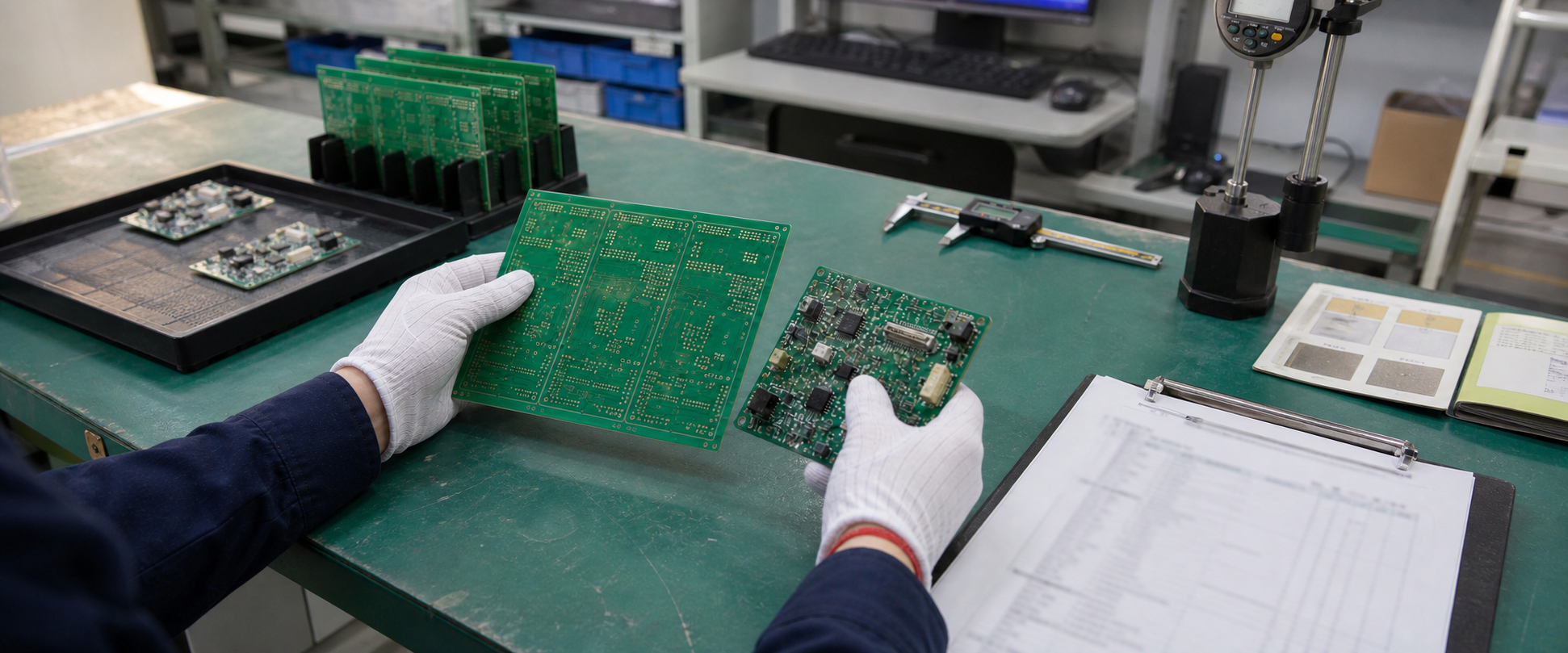
| Layer Count Capabilities | 1 - 8 Layers | Premium rigid PCB manufacturing across single-sided, double-sided and multilayer configurations. |
PCB Fabrication & PCBA Assembly Capabilities
| Parameter | Manufacturing Capabilities | Notes |
|---|---|---|
| Layer Count Capabilities | 1 - 8 Layers | Premium rigid PCB manufacturing across single-sided, double-sided and multilayer configurations. |
| Parameter | Manufacturing Capabilities | Notes |
|---|---|---|
| Supported Substrate Types | FR-4, FR-1, FR-2, CEM-1, CEM-3, aluminum-core/metal-core and high-frequency laminates (hydrocarbon- or PTFE-based). | Rigid FR/CEM, metal-core and high-frequency materials are available within the confirmed project range. FR-1/FR-2/CEM grades mainly support single-sided boards; aluminum-core constructions provide a board-level thermal path; RF materials are selected by frequency, loss and design requirements. |
| Base Material Brands | Shengyi, Kingboard, Nanya, Guoji, etc. | Specialty and high-frequency laminates, including Rogers, Taconic, and Panasonic, are available by project review. |
| TG (Glass Transition Temp) | TG130 / TG150 / TG170 | Standard options include Tg 130/150/170. Higher-Tg and other thermal-performance grades are available through material selection and engineering review. |
| Parameter | Manufacturing Capabilities | Notes |
|---|---|---|
| Max. Board Size | 546 × 650 Mm | For panel (PNL) dimensions approaching the maximum limit, specialized engineering layout is implemented to ensure manufacturing uniformity. |
| Min. Board Size | 4 × 4 mm | For boards below 70 × 70 mm, early panelization review is recommended to improve bare-board handling and, where assembly is selected, production-line efficiency. Rails, breakaways and depaneling follow the approved route. |
| Board Thickness Range | 0.5 mm – 3.0 mm | Flexible thickness options support diverse mechanical structures and application requirements. |
| Min. Core Thickness (Multilayer) | ≥ 0.2 mm (Excluding Copper) | Minimum published core thickness; dielectric performance and mechanical behavior depend on the complete approved stack-up and selected material system. |
| Finished Board Thickness Tolerance (D) | D < 1.0mm: ±0.1mm D ≥ 1.0mm: ±10% |
E.g. T=1.6mm → actual 1.44–1.76mm (±10%); T=0.8mm → actual 0.7–0.9mm (±0.1mm). |
| Inner Layer Copper Thickness | 0.5 oz - 2 oz |
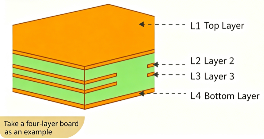 |
| Outer Layer Copper Thickness | 0.5 oz - 3 oz |
|
| Solder Mask LPI Colors Supported | Green, Blue, White, Black, Red, Yellow |
Standardized on Liquid Photoimageable (LPI) ink formulations. Matte variants or custom colors can be evaluated upon request. 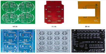 |
| Warpage (Bow & Twist) | ≤0.75% |
| Parameter | Manufacturing Capabilities | Notes |
|---|---|---|
| Mechanical Drilling (Hole Size) | 0.2 mm – 6.5 mm | Larger openings are processed by CNC routing or milling. |
| Aspect Ratio | ≤ 8:1 | The ratio of finished board thickness to minimum drilled hole diameter. E.g., for a 1.6 mm board, the minimum drillable hole is 0.2 mm. Higher aspect ratios require engineering review. |
| Mechanical Drilling (Hole Tolerance) | PTH:±0.075 mm NPTH:±0.05 mm |
Supports the specified component-lead fit or mechanical interface and helps preserve the intended soldering window; final solder fill also depends on hole design, finish, lead geometry and assembly process. |
| Mechanical Drilling (Positional Tolerance) | ±0.075 mm | Helps maintain drill-to-pad alignment and annular-ring margin against the released CAM data. Final ring condition also reflects pad design and layer registration. |
| Layer-to-Layer Registration | ±0.05 mm (±2 mils) | Controlled through optical alignment, tooling and lamination; X-Ray verification is used where the construction or control plan requires additional internal evidence. |
| Slotted Holes | Min. Slot Width: ≥ 0.5 mm |
Processed using standard mechanical CNC routing bits. Slot widths below 0.5 mm require custom engineering review. 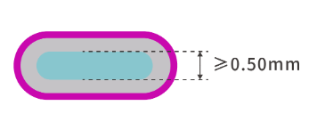 |
| Slotted Holes | Min. Slot Length: 1.0 mm (Slot length is recommended to be ≥ 2x slot width) Example: When slot width is 0.6 mm, slot length must be≥ 1.2 mm. |
If the value is below this limit, after the first hole of the slot is drilled, the remaining section will be partially unsupported. This uneven stress can cause drill deflection, leading to a misaligned or deformed slot. 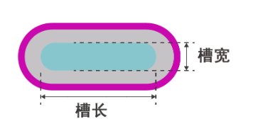 |
| Castellated Holes | Half Hole Diameter > 1.0 mm Hole-to-Hole Spacing > 1.0 mm |
Requires specialized secondary drilling and outer profile routing to ensure clean copper walls without residual burrs or lifting pads. 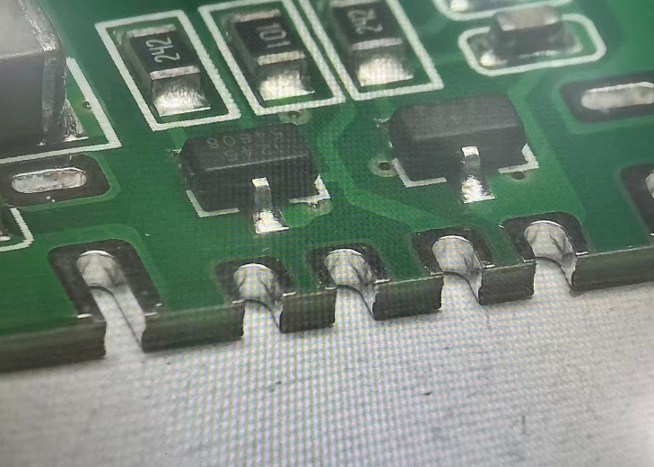 |
| Countersink Holes | Depth Tolerance: ±0.2 mm Countersink Diameter Tolerance: ±0.2 mm Standard Angle: 90° |
Please specify the drilling entry side (Top/Bottom) and target screw specifications in design files to ensure accurate depth execution. 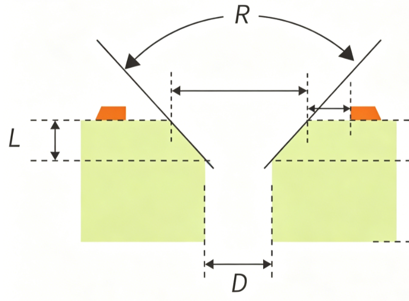 |
| Parameter | Manufacturing Capabilities | Notes |
|---|---|---|
| Hole Wall Copper Thickness | Minimum Single Point: 18 μm Average Value: 20 μm (Per IPC-6012 Class 2 Standard) |
Default: IPC-6012 Class 2. Class 3: by project agreement. |
| Parameter | Manufacturing Capabilities | Notes |
|---|---|---|
| Min. Trace / Space | 1.0 oz: ≥ 4/4 mil 2.0 oz: ≥ 5/5 mil 3.0 oz: ≥ 8/8 mil |
Minimum features are tied to base-copper thickness; CAM compensation and controlled etching help preserve released conductor geometry and reduce undercut-related variation. 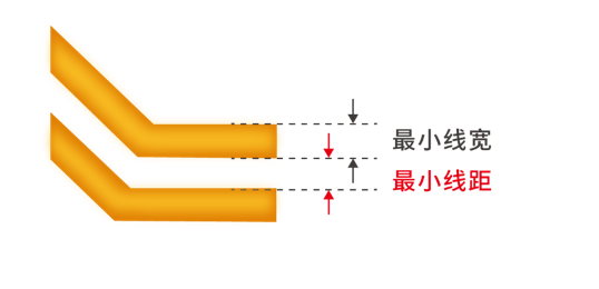 |
| Pad to Trace Clearance | ≥ 0.1mm |
The published 0.1 mm is a fabrication reference that helps control residual-copper and shorting risk; electrical spacing is finalized against voltage, material, environment and design requirements. 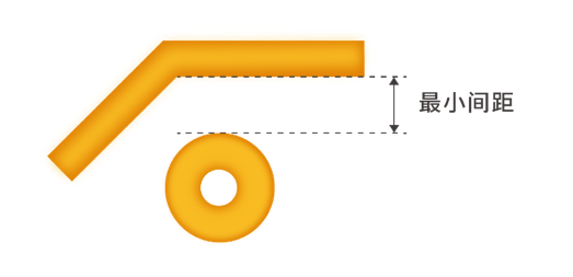 |
| Standard Trace / Space Tolerance | ±20% | Regulated via high-precision chemical etching lines. |
| Impedance Control Tolerance | ±10% | TDR coupon testing; reports available upon request. |
| Via Annular Ring Size | ≥ 0.10 mm per side (Standard) |
The published annular-ring margin helps reduce breakout risk and supports plated-hole continuity; final reliability also depends on hole structure, plating and use conditions. 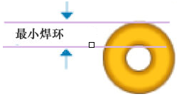 |
| Component Hole Annular Ring Size | ≥ 0.20 mm per side (Standard) | Larger annular rings can improve mechanical margin and current distribution; required dimensions depend on the lead, hole, copper and assembly design. |
| Parameter | Manufacturing Capabilities | Notes |
|---|---|---|
| Solder Mask Coating Thickness | Trace Surface: ≥ 10 μm Trace Corners: ≥ 5 μm Base Laminate: 20 - 40 μm |
Controlled coverage supports conductor insulation, edge protection and environmental durability; final performance also reflects geometry, ink system and end use. 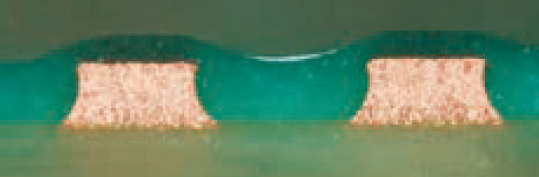 |
| Solder Mask Opening / Solder Mask Clearance | Solder mask opening ≥ 3 mil per side relative to the pad | |
| Min. Solder Mask Dam / Bridge Width | LPI: ≥ 4.0 mil (0.1 mm) |
When copper thickness ≥ 2 oz, LPI requires ≥ 7mil; for non-standard colors (non-blue/green), an additional 1-2mil is required. 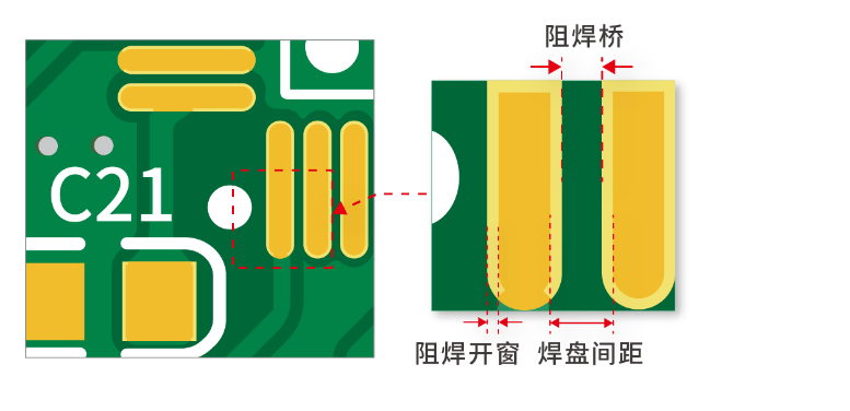 |
| Solder Mask Via Plugging Capacity | Standard Via Diameter < 0.5 mm |
Vacuum-pressure plugging with a dedicated aluminum stencil is available within the published via range, helping achieve controlled fill consistency and reduce trapped-solder or solder-ball risk. Final fill and acceptance criteria follow the approved design and order.  |
| Parameter | Manufacturing Capabilities | Notes |
|---|---|---|
| Silkscreen Legend Thickness | ≥ 10 µm | High-contrast, non-conductive screen-printing legend inks. |
| Legend Ink Colors | Black, White | In-stock inventory standard formulations. |
| Min. Legend Line Width | ≥ 5 mil | Text designed with line widths below 5 mil may experience blurring or broken strokes during screen printing. |
| Min. Legend Height | ≥ 1mm |
Special fonts, Chinese characters, and hollow text may require a larger height depending on the design. 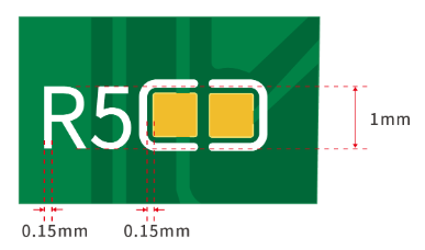 |
| Laser Marking QR Code Size | Laser marking area: ≥ 4 × 4 mm, subject to code content and readability. | Requires placement on bare laminates areas or dedicated solder mask clear zones. Optional laser-marked QR identification is available on suitable PCB designs where code content, marking area and readability have been confirmed. Traceability depth follows the agreed project scope and available production records. |
| Parameter | Manufacturing Capabilities | Notes |
|---|---|---|
| CNC Routing Profile Tolerance | Trace/Pad to Routed Edge Clearance ≥ 0.2 mm Routing Profile Tolerance: ±0.2 mm (Standard Routing), ±0.1 mm (Precision Routing) |
Stricter tolerances require special engineering control 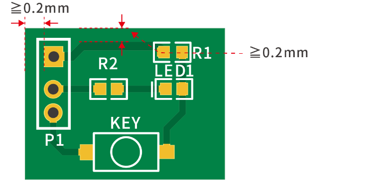 |
| V-CUT/V-Score Residual Web Tolerance | Trace/Pad to V-Score Line Clearance ≥ 0.4 mm V-Score Outline Tolerance: ±0.2 mm V-Score Residual Web Tolerance: ±0.1 mm |
Critical parameter balancing board rigidity and manual depaneling. Prevents premature breakout. 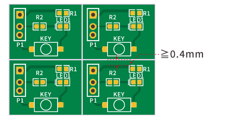 |
| Hard Tooling Punching Tolerance | ± 0.1 mm | Configured for high-volume high-speed metal punching matrix tooling. |
| Array Interface Design Rules (Breakaways) | Supports CNC, V-CUT, Bridge with Projection, Stamp Holes (4 holes per cluster standard) |
Break-away tabs and stamp-hole clusters are arranged during CAM panelization to help control residual burrs and reduce mechanical risk to nearby edge features when the specified clearance is maintained. 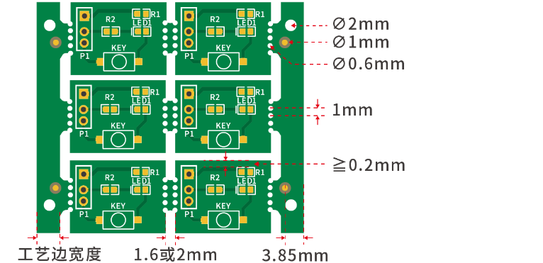 |
| Parameter | Manufacturing Capabilities | Notes |
|---|---|---|
| Leaded HASL / Lead-Free | Coating thickness: 2.0–40 μm, subject to agreed finish specification. | High-Contrast, Non-Conductive Screen-Printing Legend Inks. |
| Electroless Nickel Immersion Gold (ENIG) | Gold (Au): 1 - 3μin Nickel (Ni):3 – 5 μm |
Flat surface finish suitable for fine-pitch assembly. Wire-bonding requirements require a separately qualified finish and project review. |
| Organic Solderability Preservatives (OSP) | Thickness: 0.2μm - 0.4μm | Flat, lead-free compatible surface finish. |
| Total Carbon Deposition Thickness | 10 μm – 30 μm | Carbon-ink printing offers a cost-conscious alternative to plated contact finishes for suitable keypad contacts, resistive features and jumper applications. Resistance, wear, contact life and end use are confirmed during project review. |


The published parameters provide a reference to SUNHOPE’s current PCB fabrication and PCBA assembly capabilities. Every project is reviewed individually, covering the relevant DFM considerations, material selection, stack-up, component compatibility, process feasibility and acceptance requirements for the scope selected. Before production release, our engineers provide practical, actionable feedback to strengthen manufacturability, support stable yield and define a controlled production route.
We recommend sharing the design data applicable to your selected scope—such as Gerber files, fabrication drawings, BOM and pick-and-place data—as early as practical. Early review helps identify manufacturability risks before tooling or line release, reduce avoidable design iterations and support a smoother transition from prototype or trial build into the agreed production stage.
The specifications published on this page are reviewed and updated on a regular basis to reflect our latest process capabilities. For requirements that exceed the listed parameters, please contact our engineering team directly for a dedicated feasibility assessment.