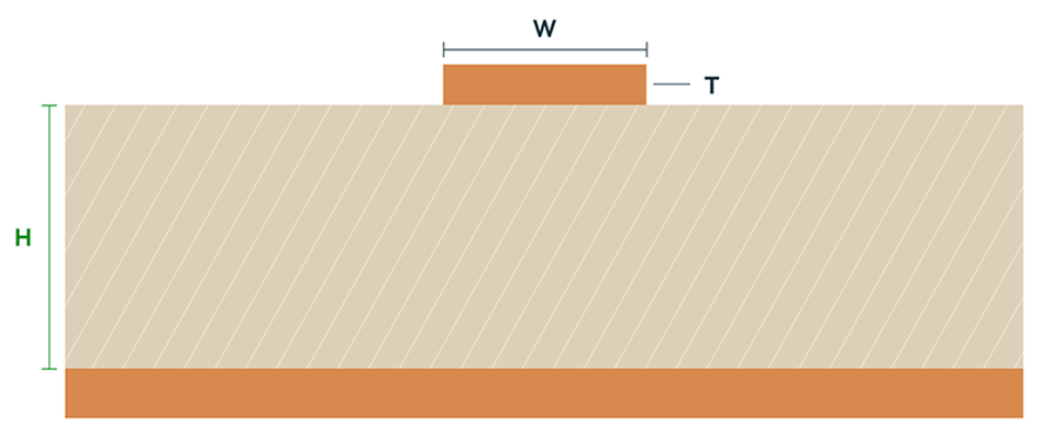
W — Trace Width
Sets the conductor's cross-section together with copper thickness — narrower traces raise impedance, wider traces lower it.

Streamlined Controlled Impedance PCB Fabrication Services
Balancing strict high-frequency performance with cost efficiency is a defining goal of modern product deployment. Within Sunhope’s confirmed 1–8 layer rigid-PCB range, suitable double-sided and multilayer controlled-impedance constructions support fast-moving commercial hardware. By funneling our entire operation into a dedicated 1-8 layer rigid production workflow, we maximize yield stability, eliminate the cost premium of ultra-high layer count production, and ensure robust interlayer connectivity. We pair traceable, high-quality base laminates with automated fabrication workflows to streamline your product's journey from rapid prototyping to volume production. Engineered to support dense BGA layouts and high-speed IoT gateways, Sunhope delivers precision controlled impedance fabrication with the pricing and delivery agility your supply chain demands.
A controlled impedance PCB is a specialized circuit board designed to manage the propagation and integrity of high-frequency or high-speed digital signals traveling along its tracks. In standard PCBs, traces function as simple electrical connections. However, in high-speed circuits, these traces act as transmission lines where the characteristic impedance (Z₀) must be precisely controlled and matched to the source and load components to prevent signal degradation. The characteristic impedance of a PCB trace is not determined by its length, but rather by its physical geometry and the surrounding insulating materials. The core of impedance control relies heavily on managing four critical parameters during manufacturing: Trace Width (W): The physical width of the copper signal track. Trace Thickness (T): The height or thickness of the copper layer. Dielectric Thickness (H): The distance or height of the insulating material separating the signal layer from the nearest reference ground or power plane. Dielectric Constant (Er / Dk): The specific electrical property of the base laminate material (such as FR-4) used between the layers. Modeling and manufacturing control of these variables help keep the produced transmission structure within the approved impedance target and tolerance. Reflections, distortion and data integrity still depend on the complete interconnect, layout, source/load matching and operating conditions.
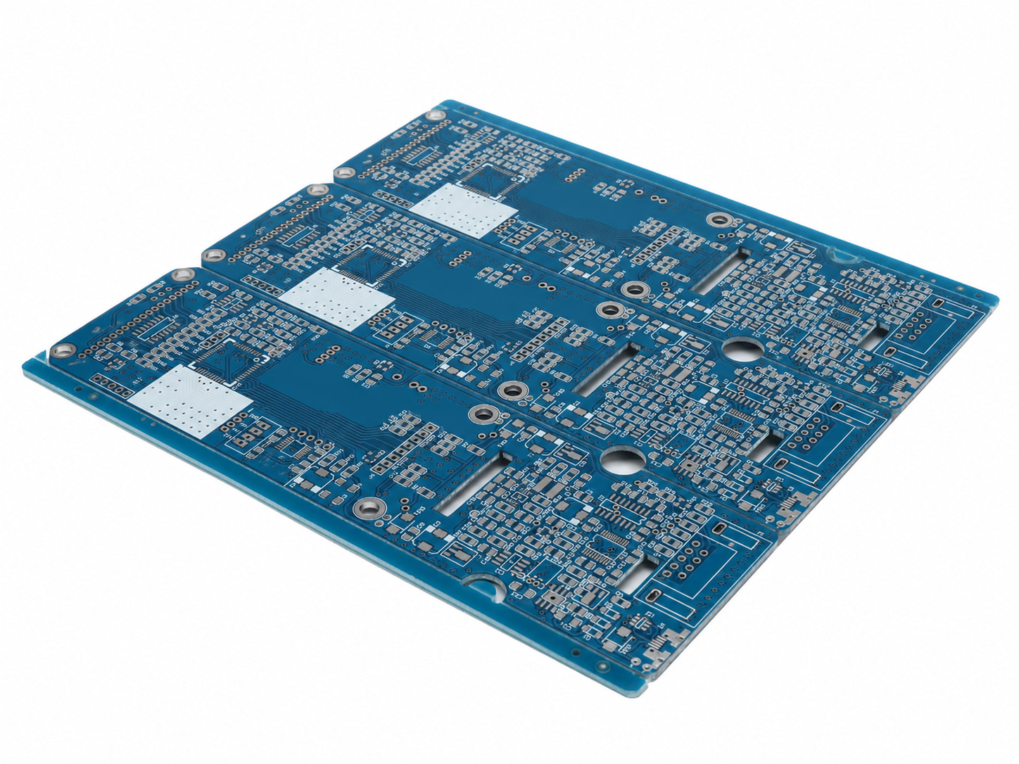 Panelized Controlled Impedance PCB
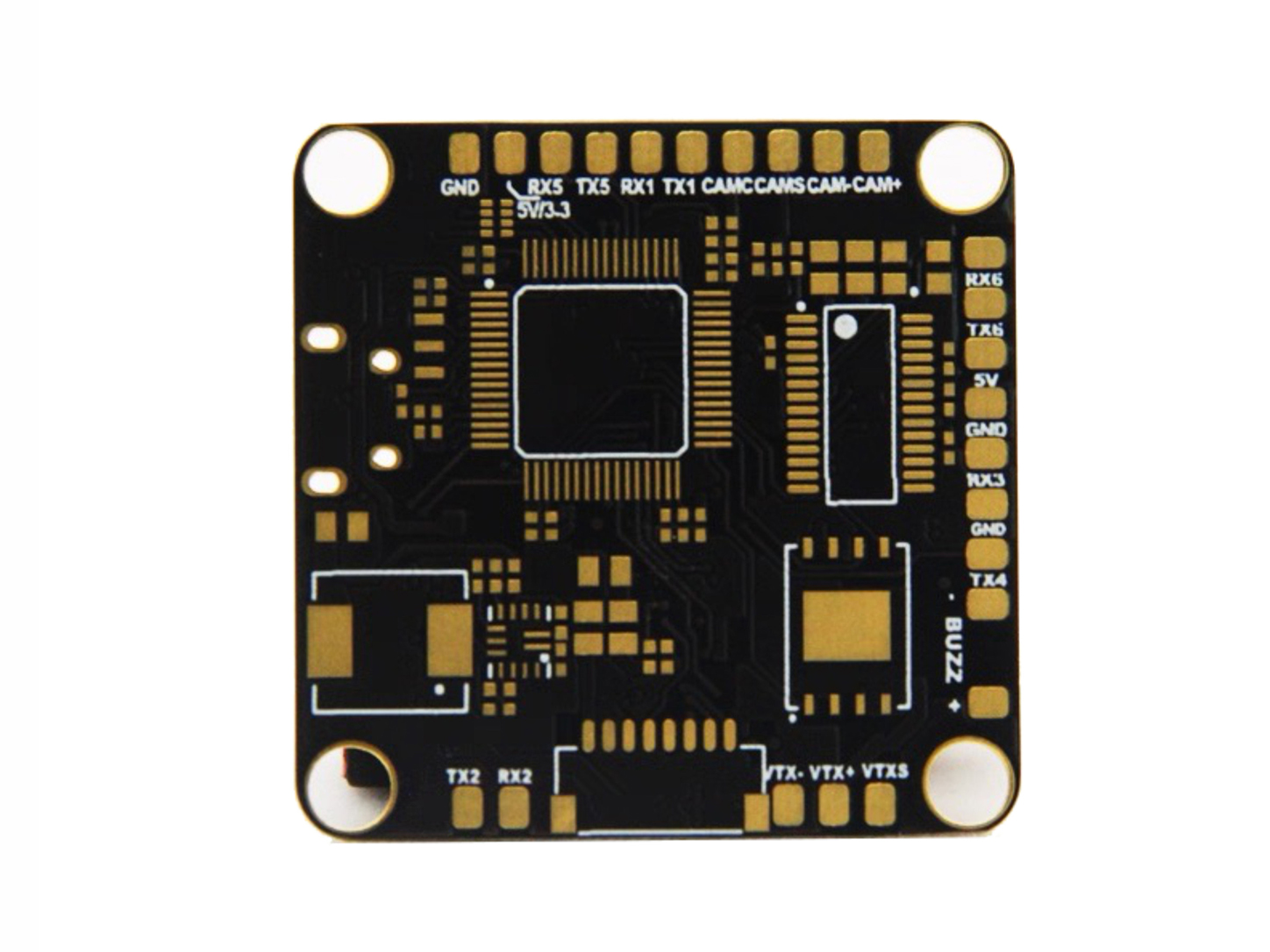 Compact Controlled Impedance PCB
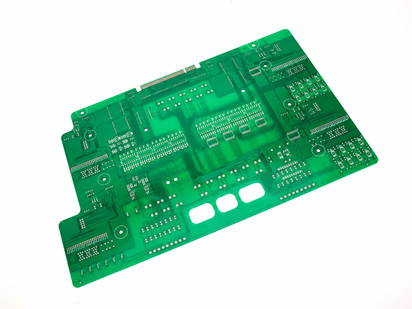 Large-Format Controlled Impedance PCB
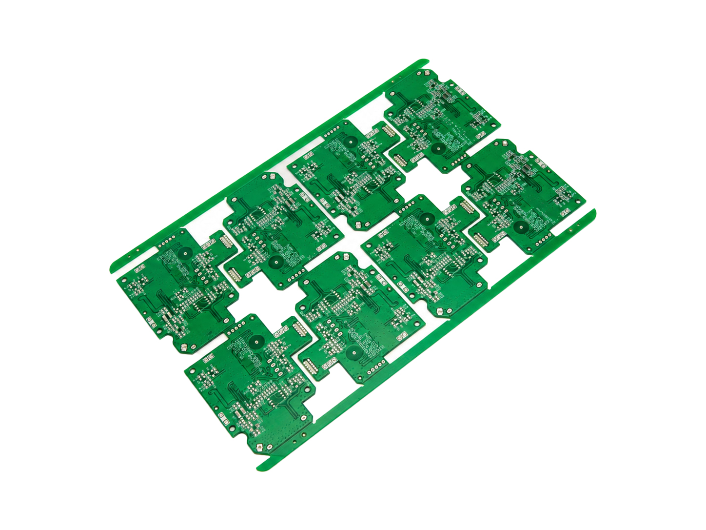 Multi-Up Controlled Impedance PCB Panel
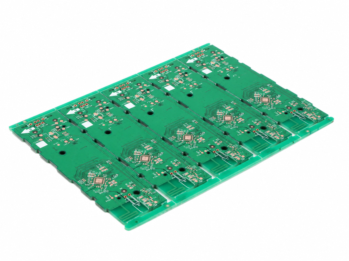 Controlled Impedance PCB Production Panel
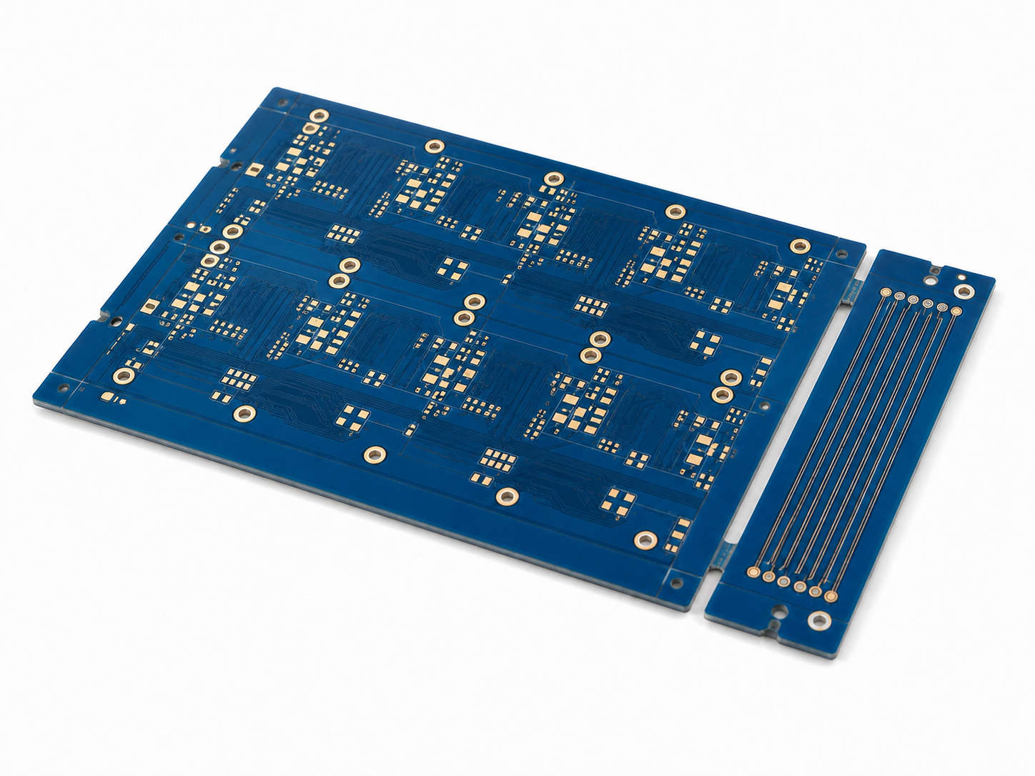 Controlled Impedance PCB Test-Coupon Layout
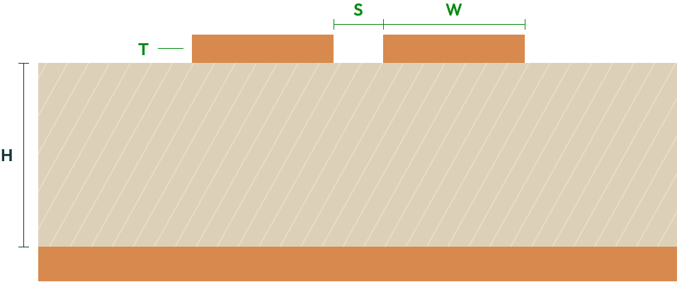
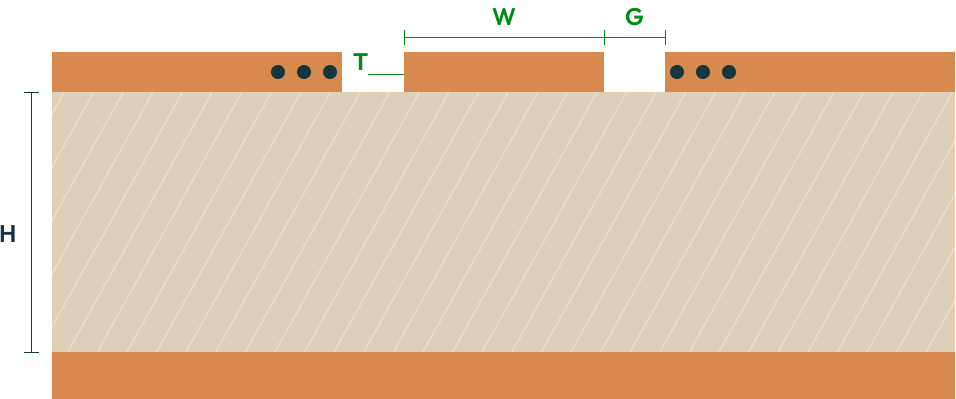
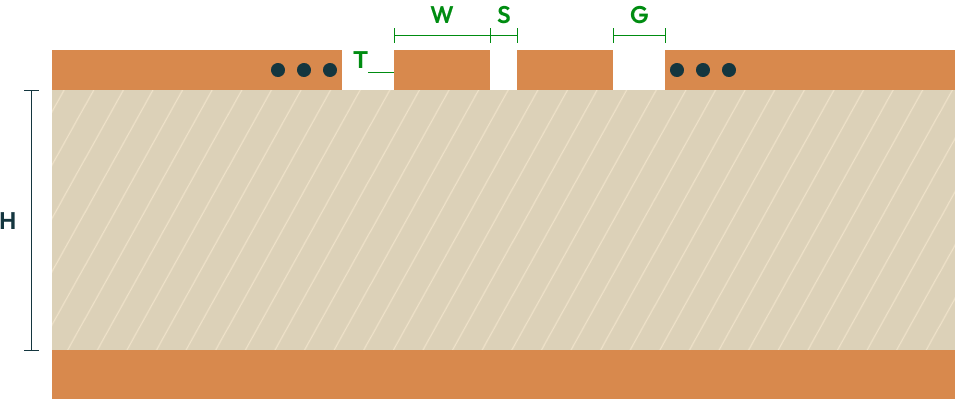
Impedance is not a standalone material property to be merely noted on a blueprint; rather, it is the physical outcome of trace width, copper thickness, dielectric height, and substrate permittivity interacting in unison. The diagrams below illustrate the precise cross-sectional geometry behind this relationship for both single-ended and differential configurations. The subsequent specification tables translate these electromagnetic dynamics into the tangible manufacturing tolerances we reliably maintain on the factory floor.
Sets the conductor's cross-section together with copper thickness — narrower traces raise impedance, wider traces lower it.
Set by the copper weight (oz) selected for that layer; factors into the same impedance calculation as trace width.
Distance from the trace to the nearest reference plane; a thicker dielectric raises impedance.
Gap between the paired traces; sets the coupling between them and determines differential impedance.
Sets the conductor's cross-section together with copper thickness — narrower traces raise impedance, wider traces lower it.
Set by the copper weight (oz) selected for that layer; factors into the same impedance calculation as trace width.
Distance from the trace to the nearest reference plane; a thicker dielectric raises impedance.
Distance from the trace edge to the adjacent ground pour on the same layer; a narrower gap increases coupling to the side ground and lowers impedance, a wider gap raises it. The pour is typically stitched to the reference plane with a via fence to keep the return path continuous.
Sets the conductor's cross-section together with copper thickness — narrower traces raise impedance, wider traces lower it.
Set by the copper weight (oz) selected for that layer; factors into the same impedance calculation as trace width.
Distance from the trace to the nearest reference plane; a thicker dielectric raises impedance.
Sets the conductor's cross-section together with copper thickness — narrower traces raise impedance, wider traces lower it.
Gap between the paired traces; sets the coupling between them and determines differential impedance.
Distance from the trace edge to the adjacent ground pour on the same layer; a narrower gap increases coupling to the side ground and lowers impedance, a wider gap raises it. The pour is typically stitched to the reference plane with a via fence to keep the return path continuous.
Set by the copper weight (oz) selected for that layer; factors into the same impedance calculation as trace width.
The distance between the signal traces and their reference plane; increasing this height generally increases impedance.
| Parameter | Specification |
|---|---|
| Impedance Tolerance | ± 10% (typical) |
| Controllable Range | 25 – 120 Ω |
| Stack-up Confirmation | Required pre-production |
| Verification Method | TDR Coupon Measurement |
| Parameter | Change | Effect on Impedance |
|---|---|---|
| Trace Width (W) | Increase | ↓ Decreases |
| Copper Thickness (T) | Increase | ↓ Decreases |
| Dielectric Height (H) | Increase | ↑ Increases |
| Trace Spacing (S, differential only) | Increase | ↑ Increases |

By matching the characteristic impedance of the trace to the source and load, it prevents signal degradation and data corruption caused by signal reflections along the transmission line.

Controlled impedance helps confine electromagnetic fields within the dielectric material, significantly reducing unwanted electromagnetic radiation and helping devices meet strict compliance standards.

Precise management of trace spacing, width, and dielectric thickness—especially in differential pairs—minimizes electromagnetic coupling and interference between adjacent signal traces.

It provides a predictable, uniform electrical path across the board, which reduces intermittent timing errors and ensures consistent, long-term performance under high-speed operation.
| Application / Interface | Signal Type | Target Impedance | Typical Tolerance | Typical Layer Count | Potential Design Impact |
|---|---|---|---|---|---|
| USB 2.0 / 3.x | Differential | 90 Ω | ±10% | 4 – 6 Layers | Data corruption, compliance test failure |
| HDMI / DisplayPort | Differential | 100 Ω | ±10% | 4 – 6 Layers | Signal reflection, display anomalies |
| Gigabit Ethernet | Differential | 100 Ω | ±10% | 4 – 6 Layers | Packet loss, link instability |
| PCIe Gen3 | Differential | 85 Ω typical | ±15% | 6 – 8 Layers | Signal degradation, eye-diagram test failure |
| DDR3 / DDR4 Memory Bus | Single-ended | 40 - 60 Ω | ±10% | 6 – 8 Layers | Insufficient timing margin, read/write errors |
| RS-485 / RS-422 | Differential | 120 Ω | ±10% | 2 – 4 Layers | Long-distance communication bit errors |
| RF / Antenna Feedline | Single-ended | 50 Ω | ±10% (Narrowband/precision RF matching may require tighter tolerance) | 2 – 4 Layers | Excessive power loss, VSWR mismatch |
Values shown are commonly referenced industry targets; final target impedance and tolerance should be confirmed against your specific design and the relevant interface specification.

Manufacturing Capabilities
To optimize your browsing efficiency, we have consolidated our verified baseline capabilities — including impedance tolerance, trace geometry and stack-up parameters — into a single reference matrix. Access our master data sheet below to review complete technical parameters across all 1-8 layer PCB products.
Access Master Capabilities & Technical Specs →To bridge the gap between electrical simulation and actual board manufacturing, applying strict Design for Manufacturing (DFM) rules is vital. Implementing these four core guidelines minimizes fabrication errors and ensures tight impedance control:
Get a Quote
Controlled impedance traces must always be routed over a solid, continuous reference plane (GND or Power). Avoid routing across split planes, slots, or voids, as any reference plane interruption causes severe impedance discontinuities, signal distortion, and electromagnetic interference (EMI).
For differential pairs (such as 90Ω USB or 100Ω Ethernet traces), maintain a constant trace width (W) and a uniform intra-pair spacing (S) along the entire signal path. Avoid sharp 90-degree corners; use 45-degree bends or smooth curves to prevent localized impedance deviations.
Keep layer transitions (vias) to an absolute minimum on critical high-speed lines, as vias introduce parasitic capacitance and inductance that disrupt Z₀. When a via is unavoidable, design a properly oversized clearance hole (antipad) in the reference planes to mitigate localized impedance drops.
When a narrow impedance-controlled trace connects to a significantly wider component land pad (such as IC pins or discrete footprints), implement a tapered trace transition. This geometric compensation smooths the abrupt capacitive change and prevents a sudden drop in impedance at the junction.
THE SUNHOPE SOLUTION
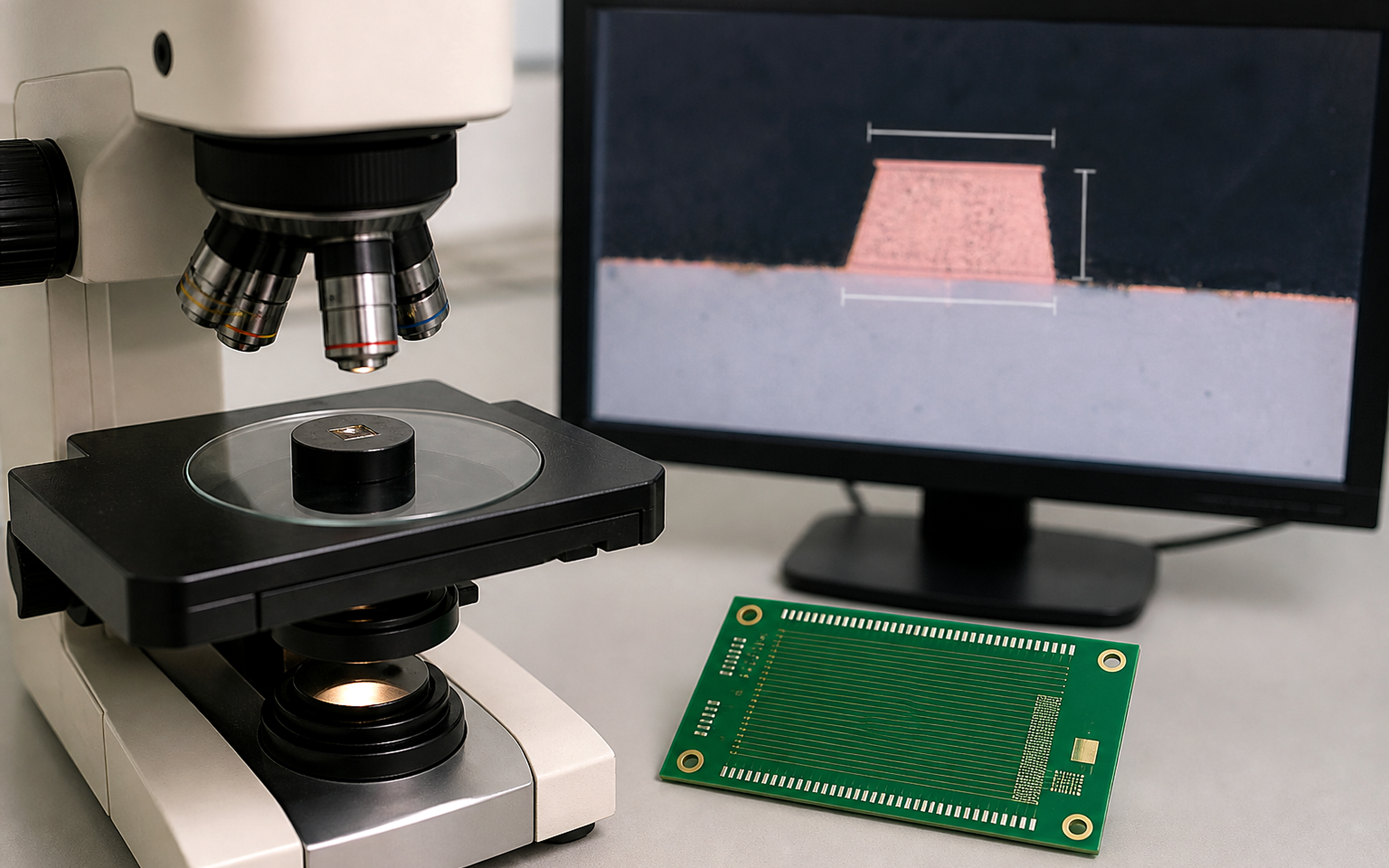
Chemical etching naturally causes lateral erosion (under-cutting), making the final copper track cross-section trapezoidal (narrower at the top than the bottom), which shifts the calculated impedance away from the target value.
CAM compensation and controlled etching are applied according to the base copper and approved fabrication data. The produced conductor geometry is checked against the released drawing and control plan; the applicable trace-width tolerance follows the copper thickness and geometry and is not equated with the published ±10% typical impedance tolerance.
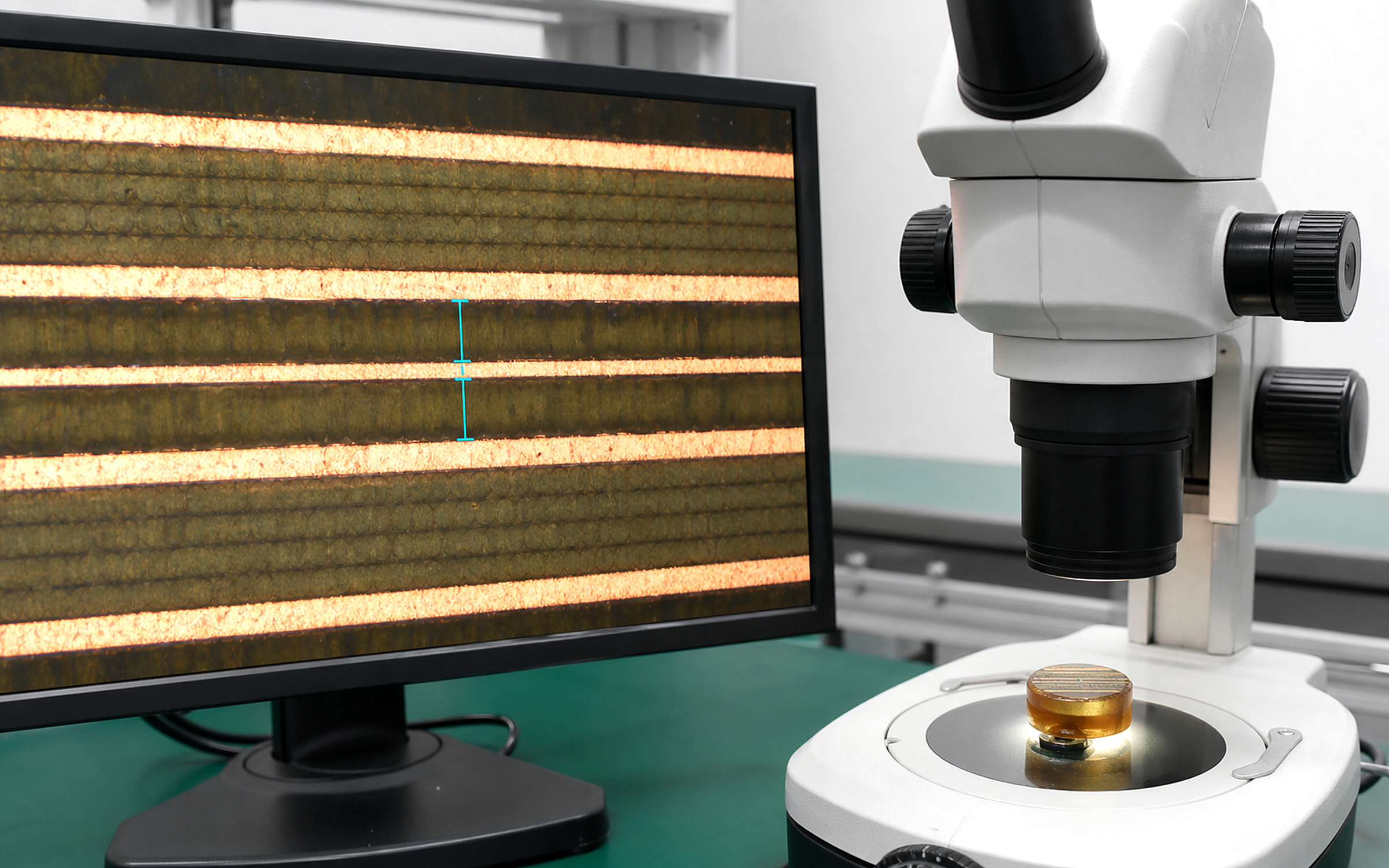
During high-pressure lamination of 4-8 layer stacks, prepreg resin flows and distributes unevenly, causing localized variations in dielectric thickness (H) and leading to sudden impedance jumps along the transmission line.
We optimize the vacuum pressing profile—precisely balancing the temperature and pressure curves—and strategically design the copper distribution of inner layers to ensure uniform resin press-out. This minimizes the structural variations inherent to the lamination process.
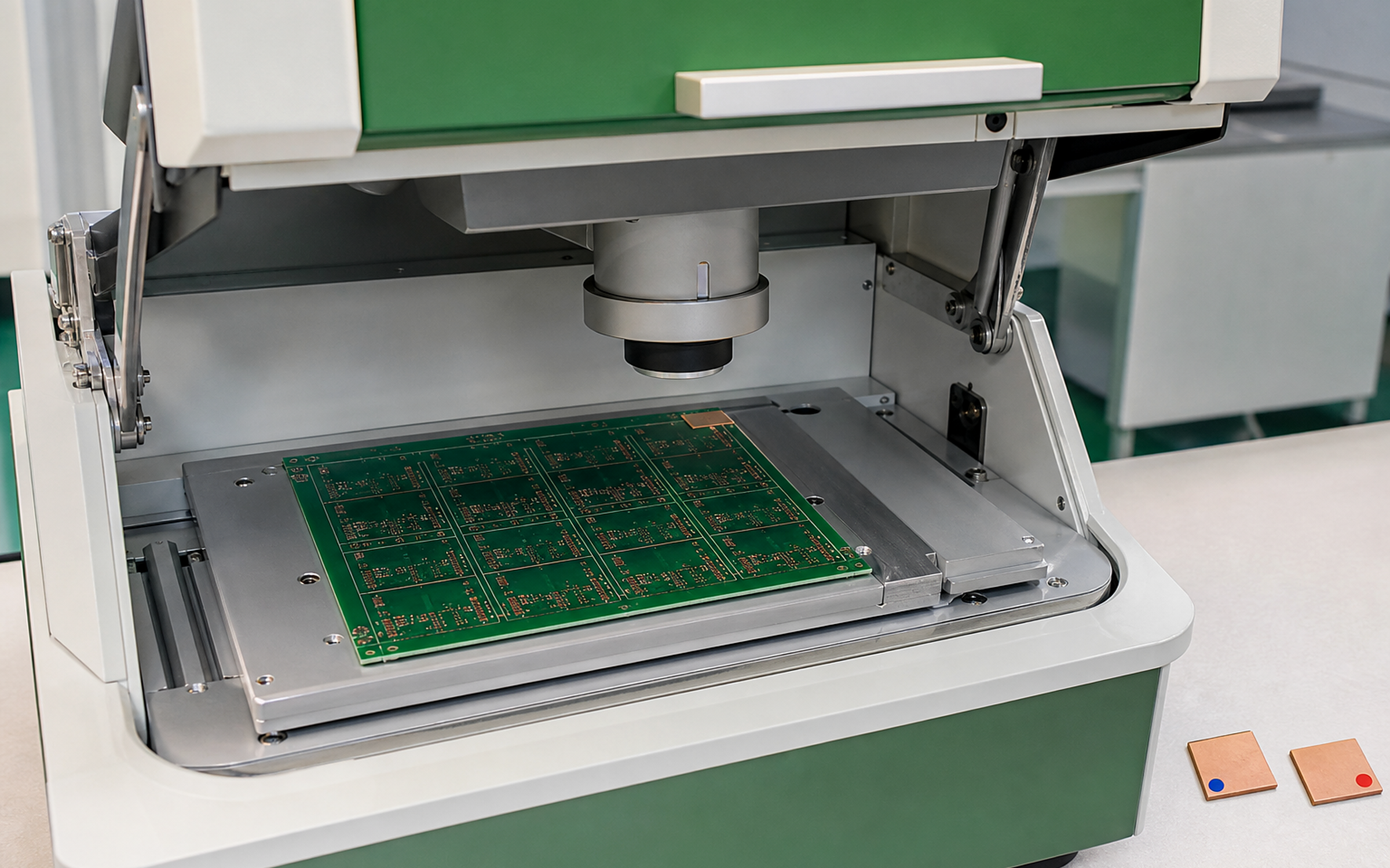
Electroplating variances can cause the outer layer copper thickness to fluctuate between the center and edges of the panel, altering the cross-sectional area of impedance tracks.
Segmented plating lines with reverse-pulse control promote more uniform copper distribution across the production panel and more predictable conductor cross-sections for specified controlled-impedance structures. Final geometry and coupon results are verified against the approved CAM data and control plan.
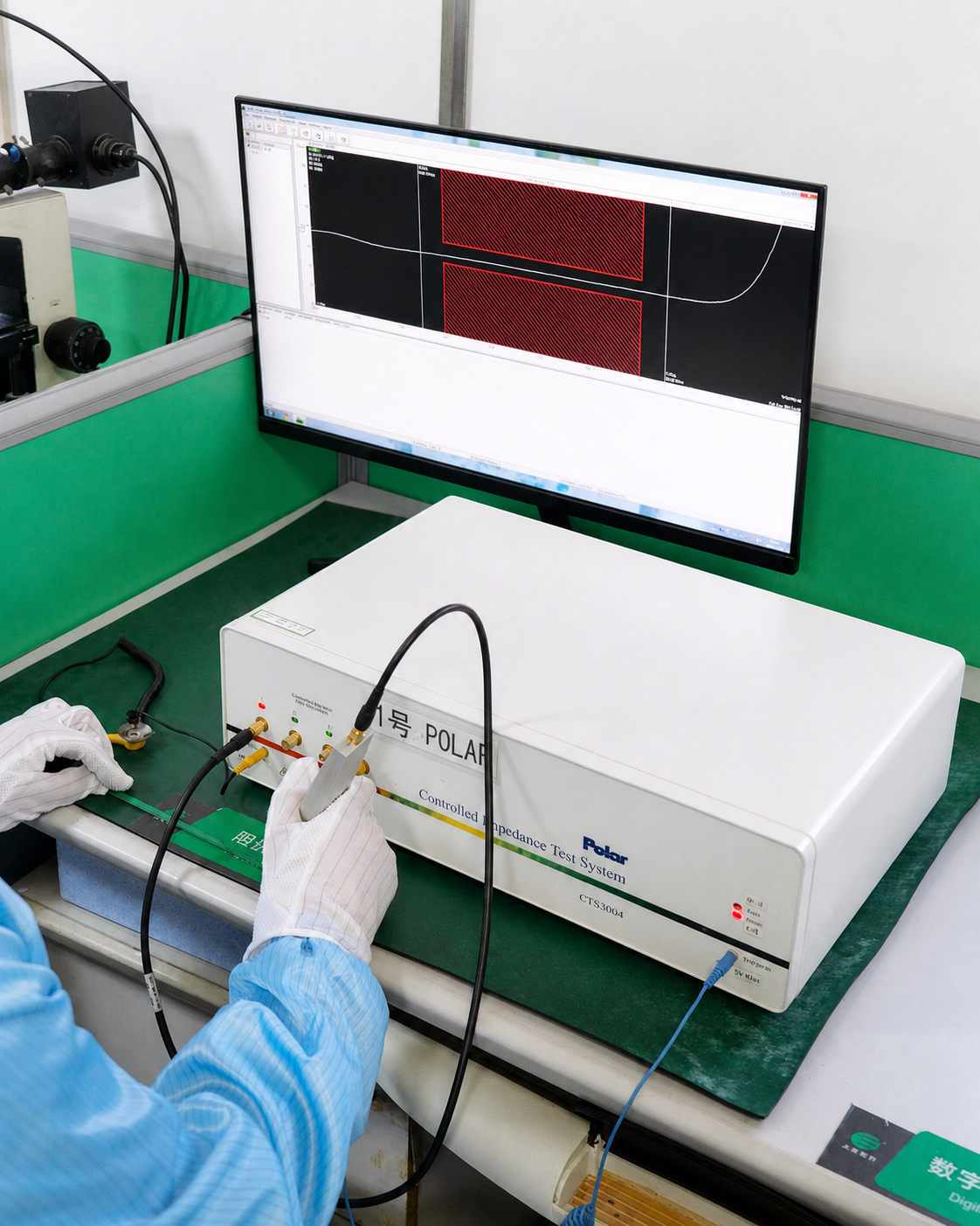
SUNHOPE verifies controlled-impedance production through a defined combination of TDR coupon measurement, physical-geometry evidence, electrical testing and lot-linked records. The method, target, tolerance, coupon representation and report scope are confirmed with the released construction:
The approved coupon set from each controlled impedance production panel is measured against the agreed target and tolerance. Results confirm the impedance represented by the stated coupon structure; they do not constitute a scan of every finished high-speed trace.
The coupon set is designed to represent the specified single-ended, differential or coplanar structures, including the relevant layer, reference plane, geometry and material build. Every specified structure represented in the approved set is included in the TDR measurement.
Production coupons or sampled sections are reviewed at the frequency defined by the control plan to verify selected copper, trace-width and dielectric characteristics. Microsection evidence supports the manufactured geometry but does not replace the electrical TDR result.
Every finished double-sided and multilayer controlled impedance PCB receives 100% netlist-based continuity and isolation testing. This detects opens and shorts in the approved network and remains separate from impedance verification.
TDR results are linked to the corresponding production lot. A customer-facing chart or report is supplied when included in the quotation or approved quality plan, so report content matches the measurement actually performed.


Target Applications of Controlled Impedance PCBs
Used in PLCs and servo drives. Precise single-ended and differential impedance ensures reliable data transmission over industrial buses (EtherCAT, CAN, Profinet) in high-noise environments.
Have more questions? Visit our Comprehensive FAQ Center for more detailed information.
View More FAQYes. For 4-8 layer configurations, we provide precision impedance control. By tightly monitoring our etching rates to minimize line-width variations and controlling dielectric thickness, we ensure that critical high-speed transmission lines stay within your targeted tolerances.
Yes. Our CAM engineering team performs comprehensive pre-production engineering reviews. We use industry-standard impedance calculation software to validate your stack-up, verify trace geometries, and provide optimization recommendations to ensure a manufacturable design before fabrication begins.
SUNHOPE’s published baseline is ±10%. Tighter tolerances can be evaluated through material, stack-up, conductor-geometry, coupon and verification review, with feasibility and commercial scope confirmed before quotation.
We optimize the vacuum press-out thermal profiles to carefully regulate resin flow during high-pressure lamination. Additionally, we deploy copper balance layout structures on inner layers to prevent local resin starvation or excess accumulation, ensuring a uniform dielectric height.
Every batch of controlled impedance PCBs undergoes 100% Time Domain Reflectometry (TDR) testing performed on the panel test coupons. This provides non-destructive, highly precise verification of the actual characteristic impedance before shipping.
A customer-facing TDR chart or report is supplied when included in the quotation or approved quality plan. The underlying measurement result remains linked to the corresponding production lot.
Yes. Share the target impedance, finished thickness, layer constraints and available mechanical requirements, and SUNHOPE’s engineers can review or propose a manufacturable 1–8 layer stack-up. This early stack-up support helps connect electrical intent with material availability and production control; the agreed engineering and commercial scope is confirmed with the project.
Yes. We can process multiple different impedance values across different layers or even on the same layer of a 4-8 layer board. You just need to clearly specify the target values and corresponding net names in your impedance table or fabrication notes.
 Q4 2026 Electronics Supply Chain Outlook for PCB and PCBA Buyers
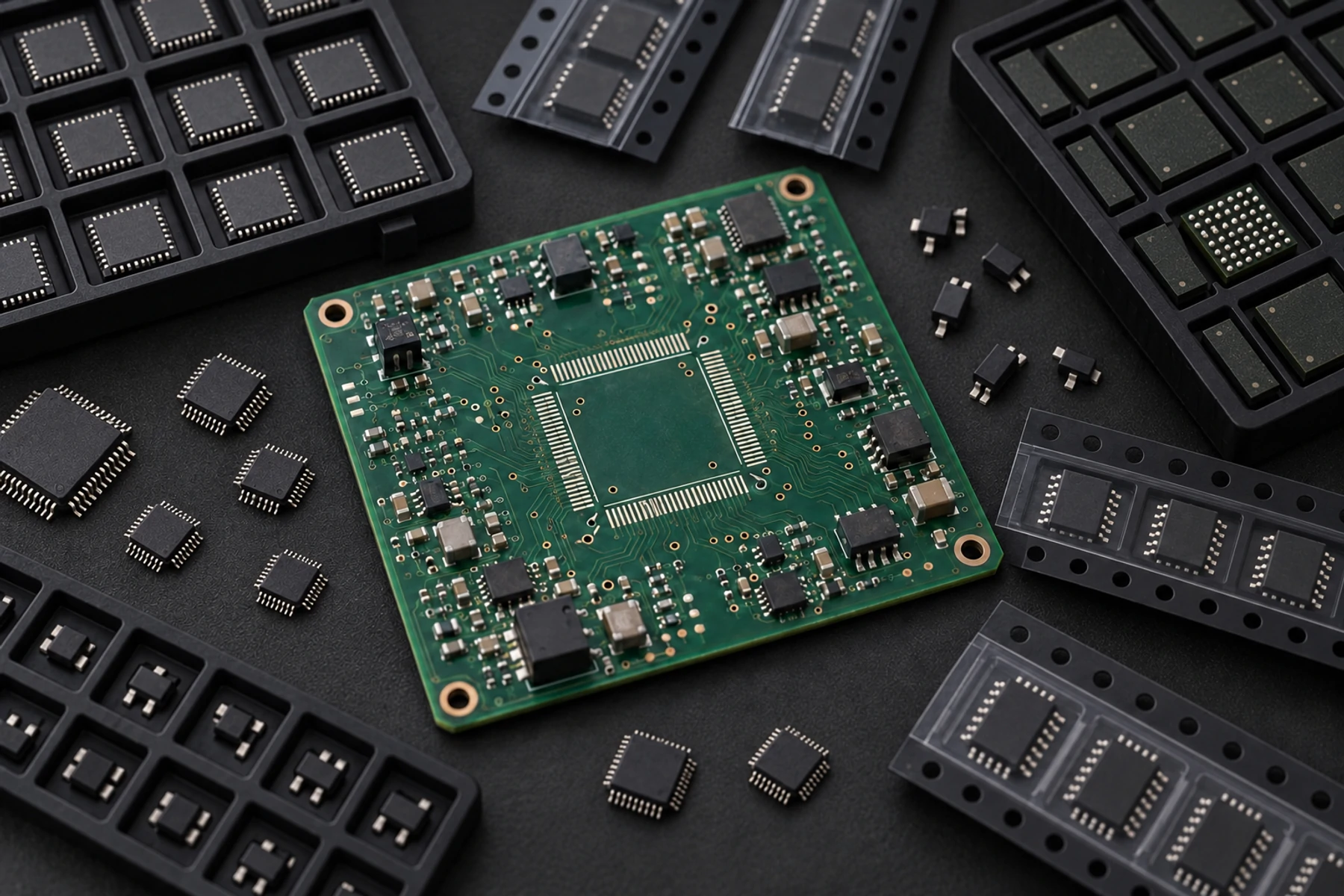 Semiconductor Market Growth Does Not Mean Every BOM Is Easy to Source
 PCB Prototype to Production-Ready PCBA: Files, Pilot Builds, Testing, and Release Control
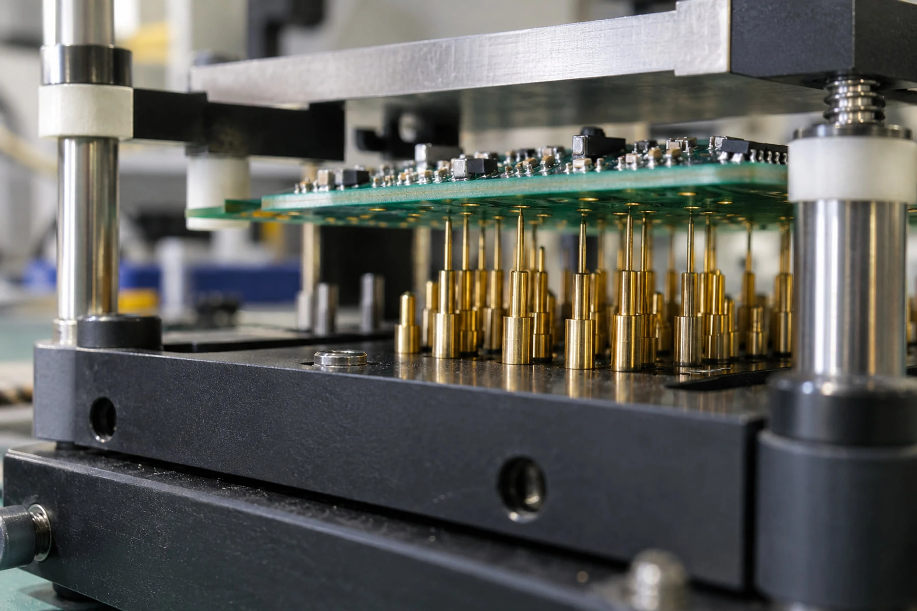 PCBA Functional Test Requirements: What Buyers and Assembly Suppliers Must Define Before Quotation
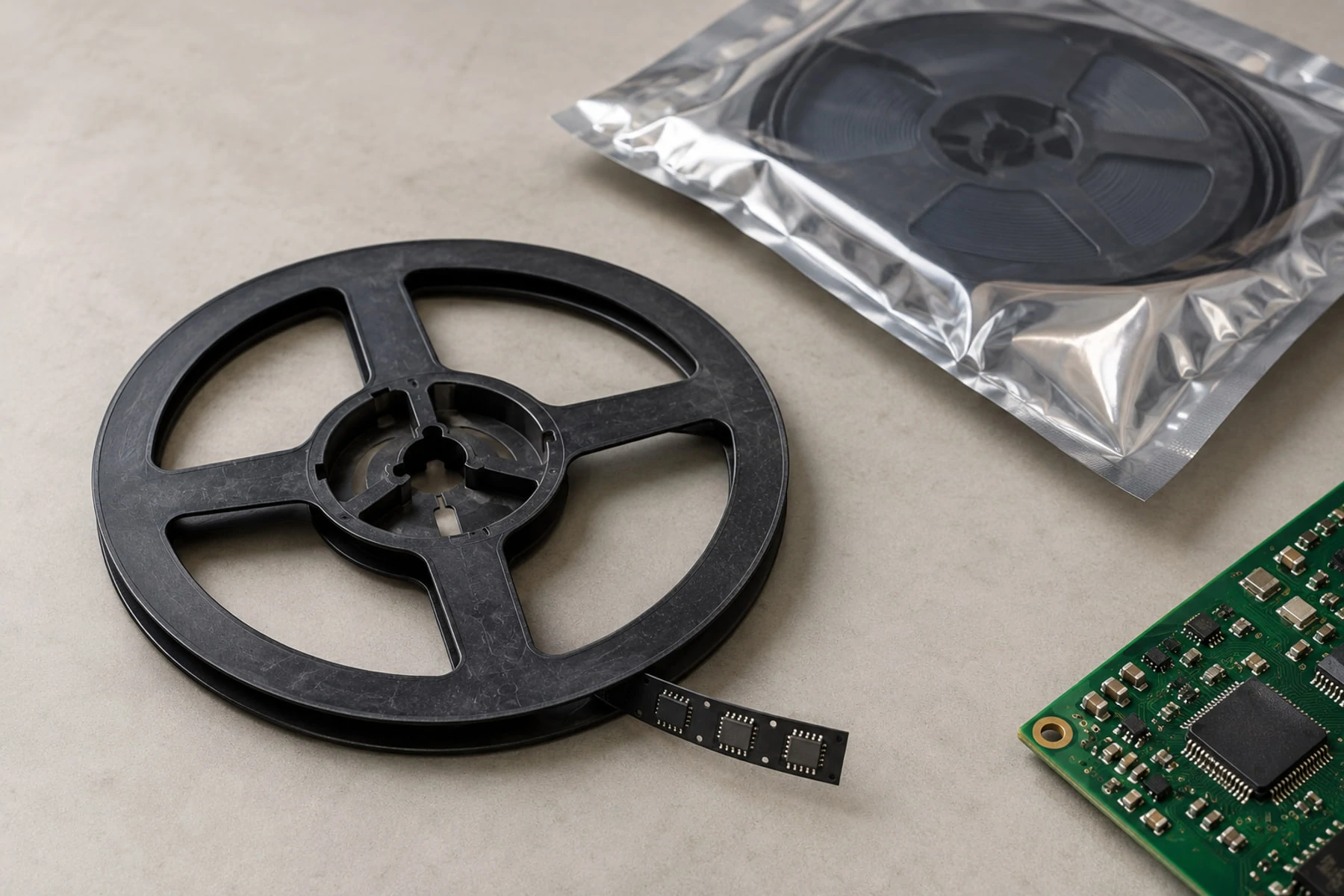 Electronic Component Obsolescence Management for PCBA Projects: From EOL Risk to Approved Change