Advanced Multilayer PCB (4-8 Layers) Manufacturing Services

Multilayer PCB

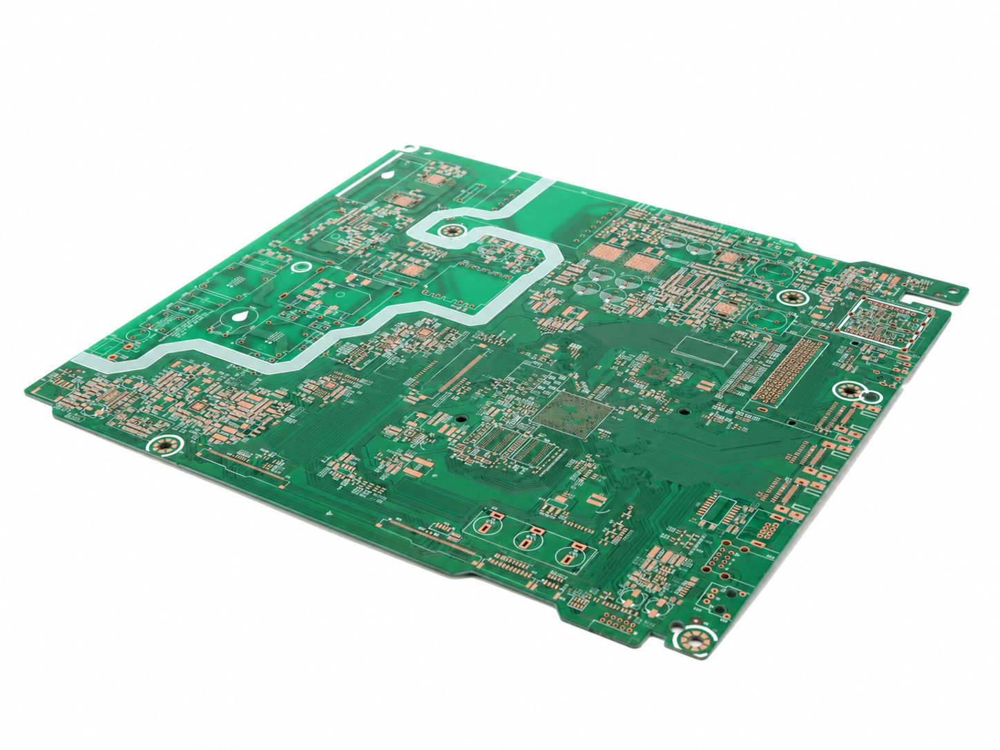
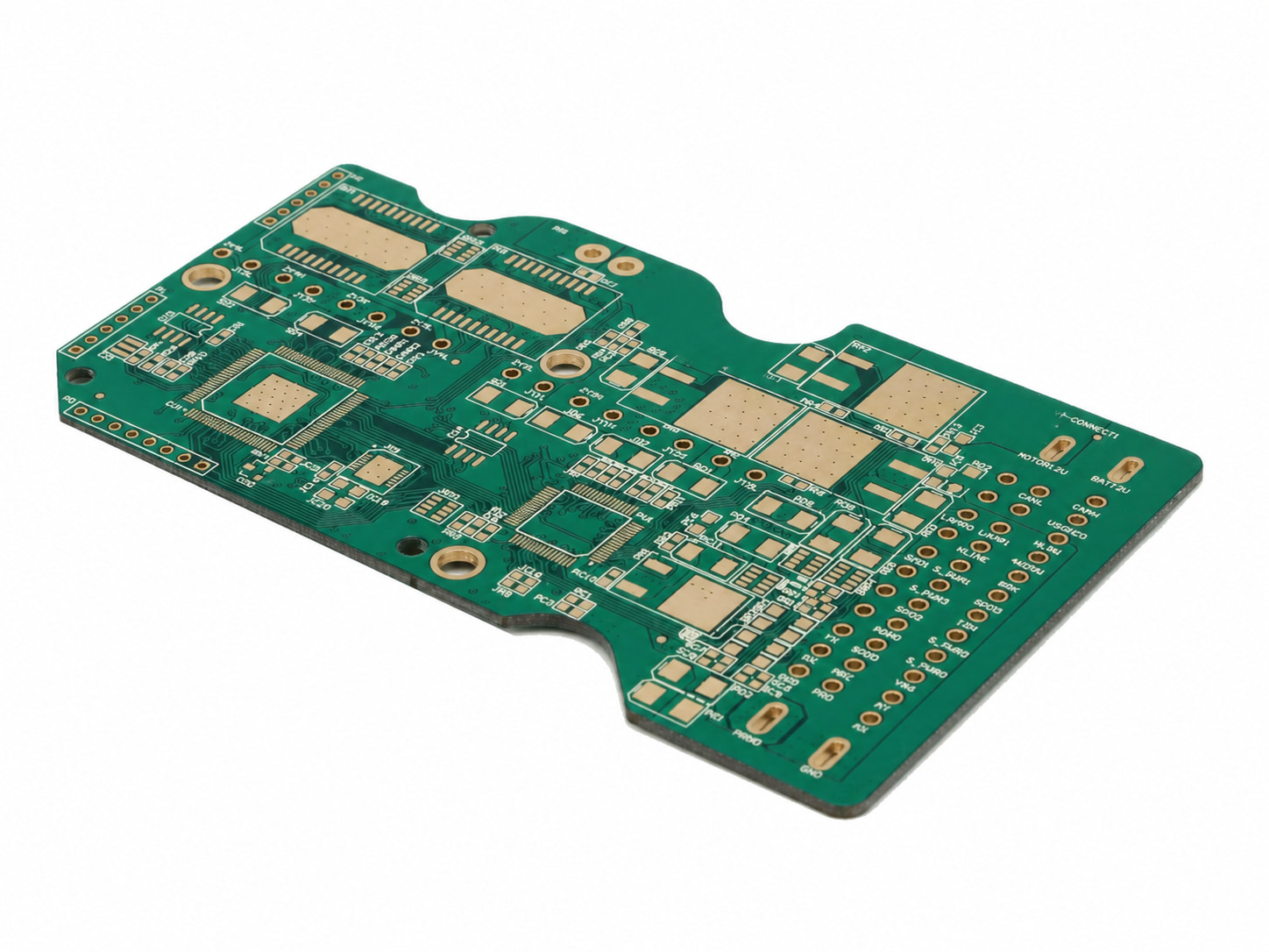
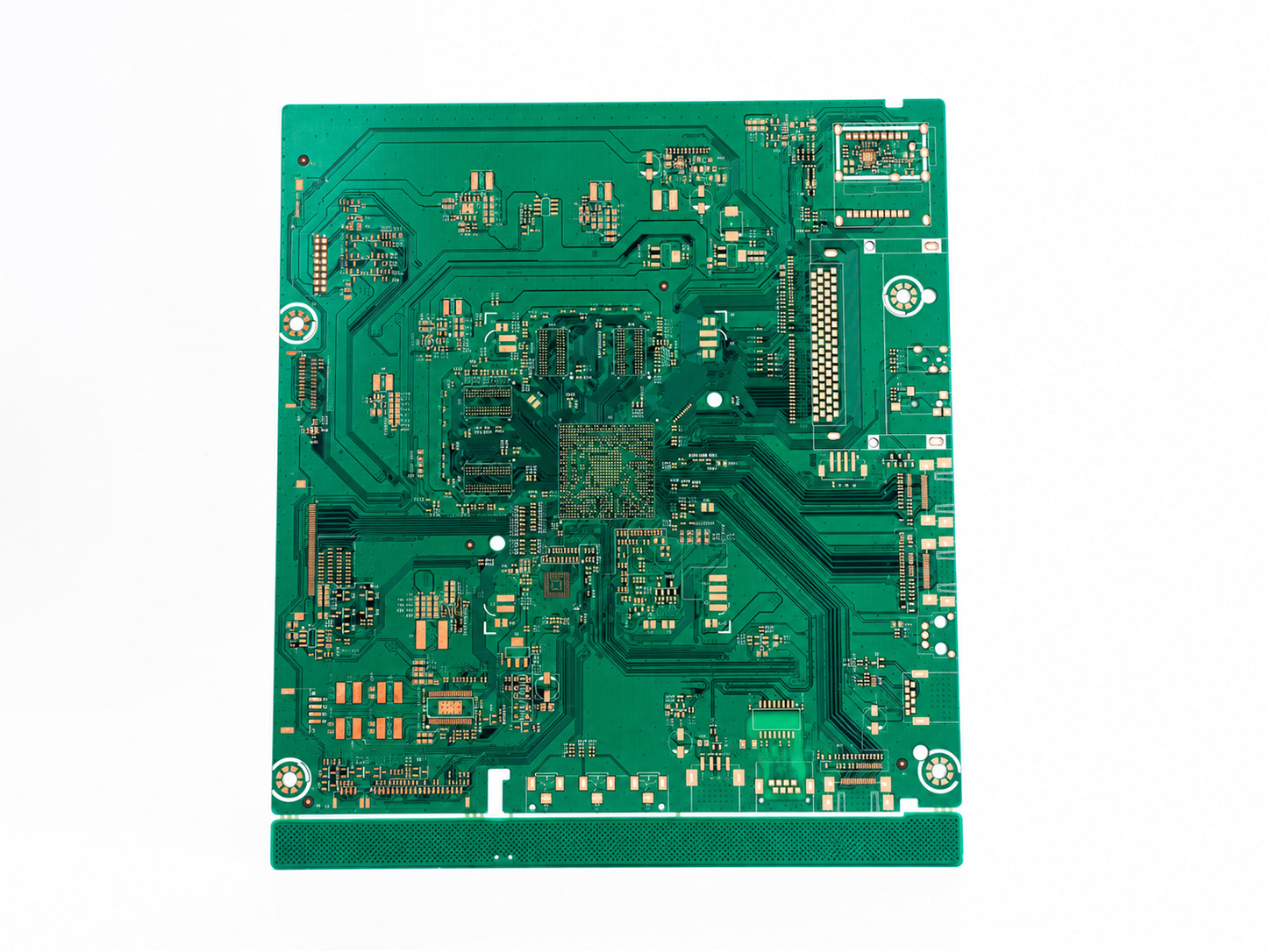
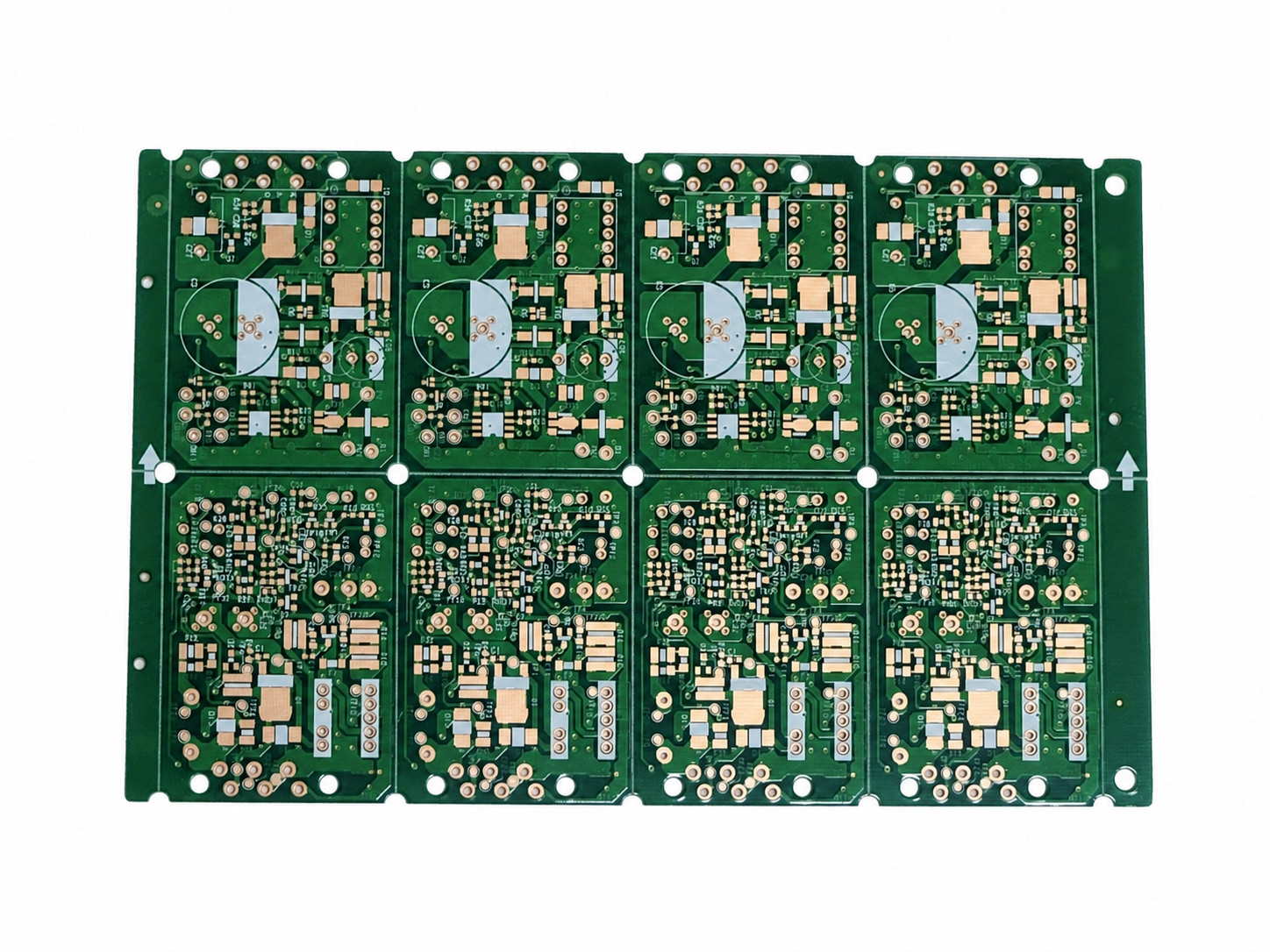
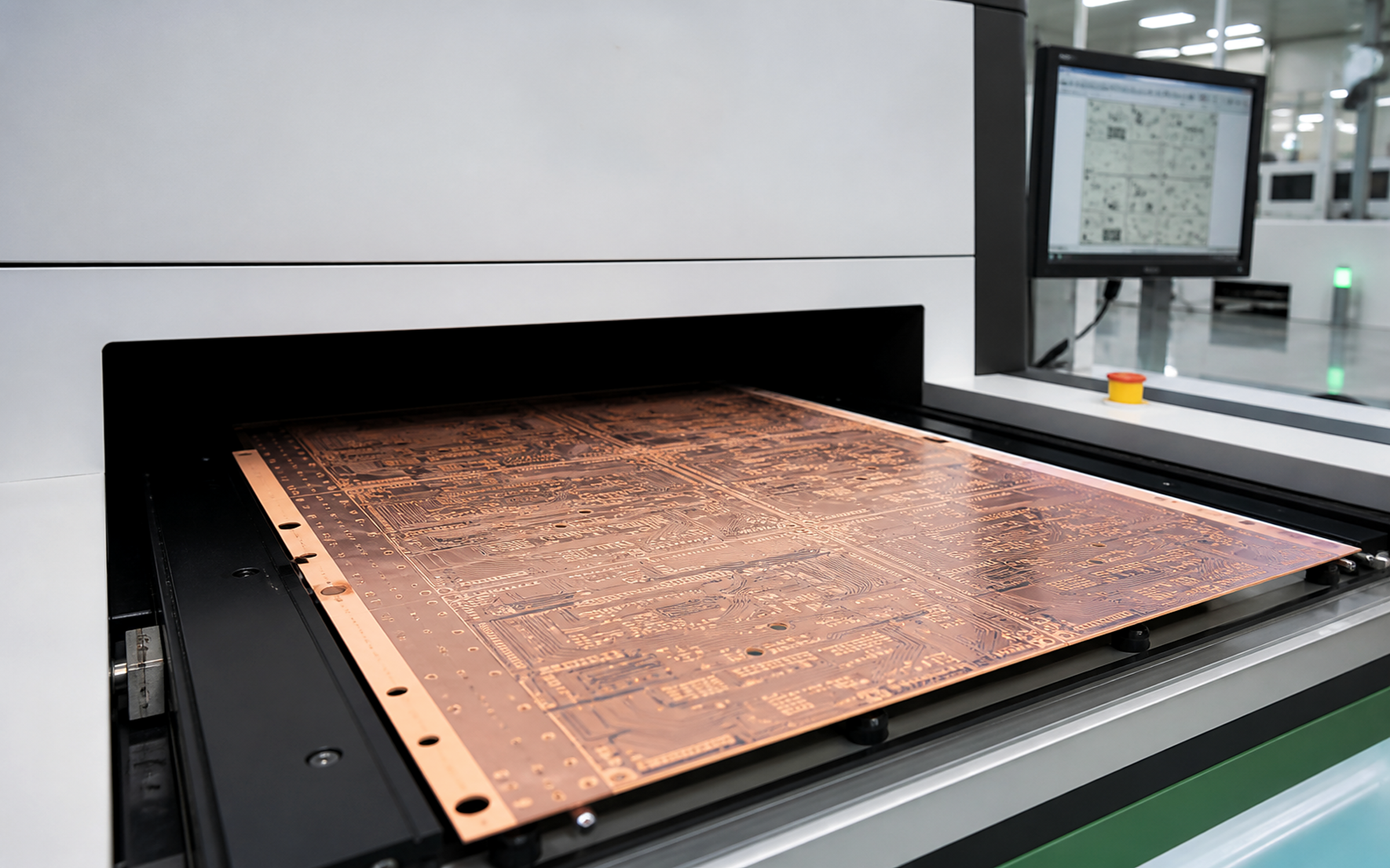
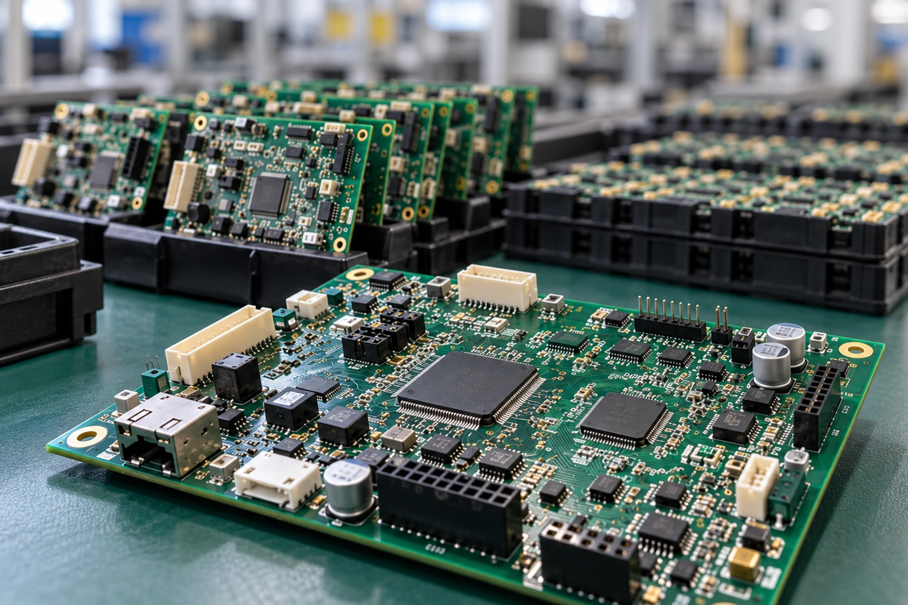
As electronic designs shift toward high-density integration and high-frequency operations, multilayer PCBs (4 to 8 layers) serve as the essential hardware foundation for managing complex inter-layer routing and critical signal integrity. Operating within our core 1-8 layer fabrication capabilities, Sunhope specializes in precision-engineered rigid multilayer PCB manufacturing and assembly services. By utilizing premium substrates—ranging from High-Tg FR-4 to specialized low-loss laminates for controlled impedance—combined with automated vacuum lamination and CCD-aligned exposure systems, we ensure stable layer-to-layer registration and robust interlayer connectivity. This layered architecture incorporates dedicated internal ground and power planes to effectively suppress electromagnetic interference (EMI) and support dense BGA layouts. Engineered for demanding industrial controls, telecommunications, automotive mainboards, and compact IoT gateways, Sunhope adapts our automated fabrication and inspection workflows to help you mitigate overseas compliance risks and streamline supply chain operations from rapid prototyping to high-volume production.
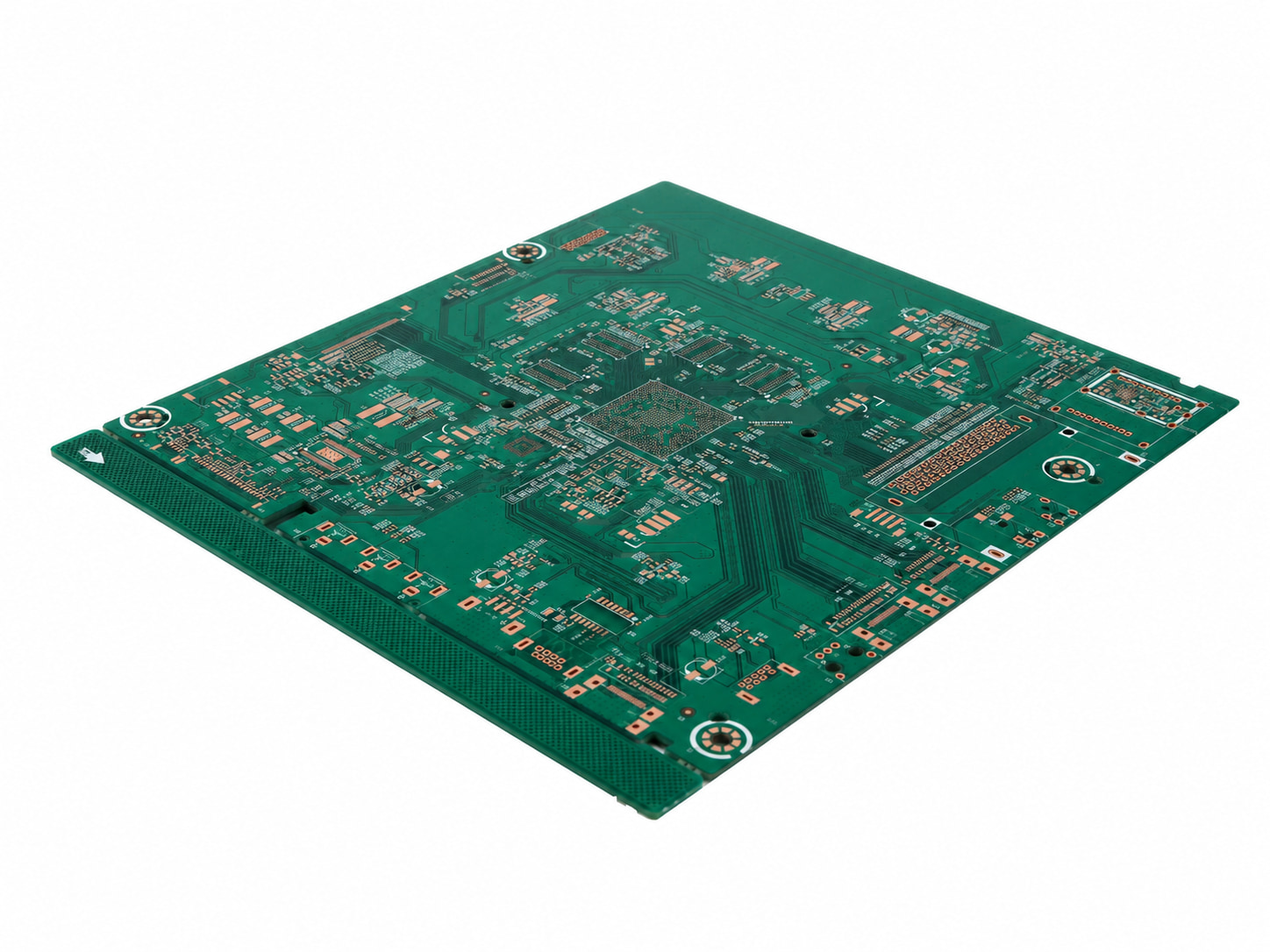
What is a Multilayer PCB?

A multilayer PCB marks the transition from two-sided routing to a deliberately structured signal, power and reference architecture. By laminating multiple copper and dielectric layers into one controlled build, it creates room for denser routing, dedicated reference planes and clearer separation of signal and power functions within SUNHOPE’s 1–8 layer rigid-PCB range. When stack-up, return paths, conductor geometry and materials are engineered together, this structure can support controlled impedance, power distribution, lower coupling risk and more disciplined EMI design. For industrial, automotive, communication and connected hardware, the value is not complexity for its own sake—it is placing each electrical function where the released design can use it most effectively.

Stack-up & Lamination

The diagrams below illustrate typical stack-up configurations for each respective layer count, with individual layers clearly labeled by material type and functional role. For optimal visual clarity, these diagrams are simplified and not drawn to actual material thickness scale; production-ready stack-ups are custom-engineered per specific design rules.

Table 1: Lamination Process Flow

StageProcess Description
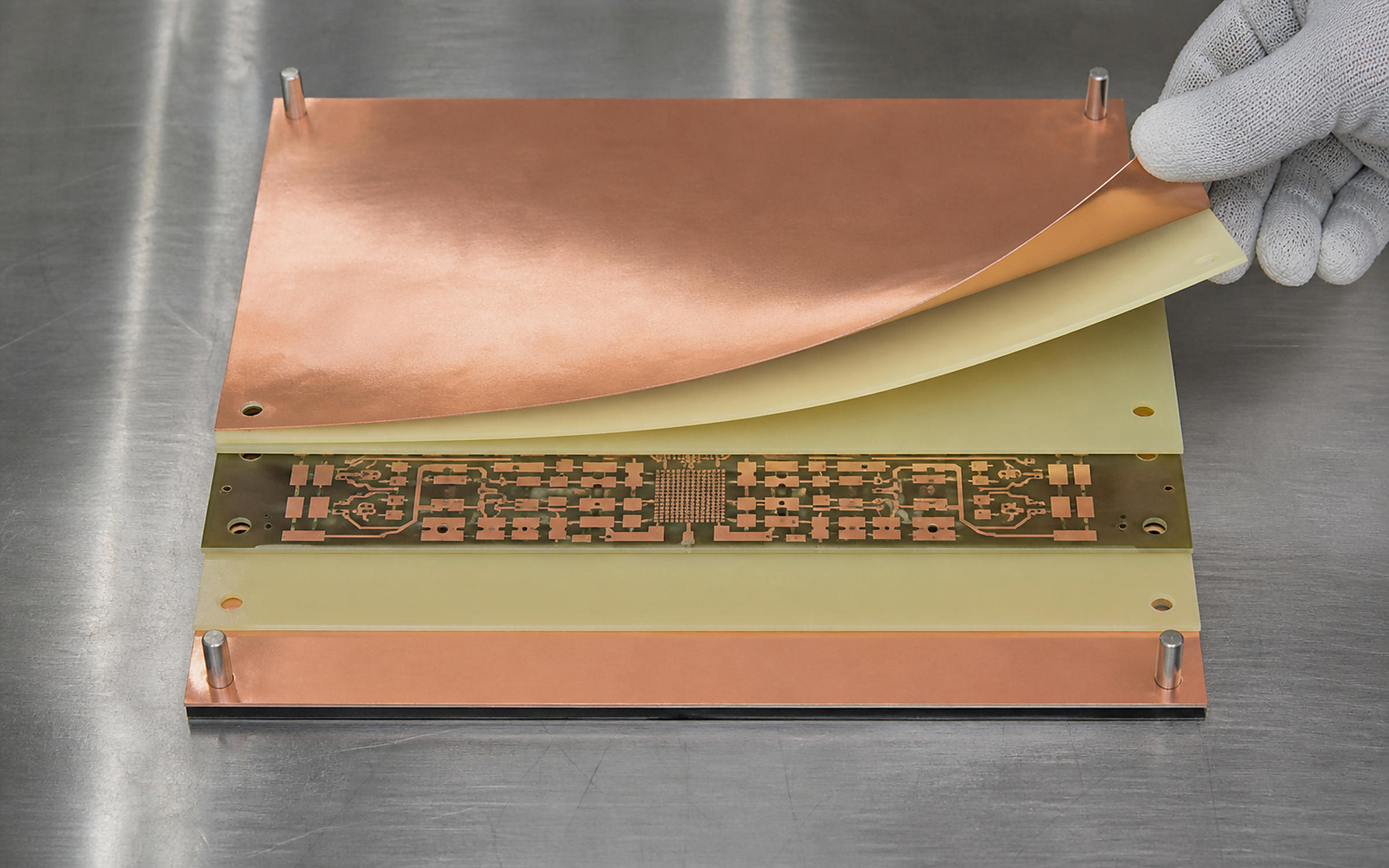
01. Stack & AlignInner layers, prepreg, and core materials are precisely stacked and mechanically aligned prior to pressing.
02. Vacuum LaminationControlled heat and pressure are applied within a high-vacuum environment to physically bond the distinct material layers uniformly.
03.Cured & BondedThe resin within the prepreg fully cures under strict thermal profiles, transforming the stacked materials into a stable, rigid multi-layer panel.

Table 2: Lamination Key Capability Parameters

Technical ParameterManufacturing Specification
Lamination MethodVacuum, controlled temp/pressure
Layer-to-Layer Registration±0.05 mm (±2 mils)
Prepreg / Core OptionsMultiple builds available
Rigid-PCB Acceptance & PTH Plating CriteriaIPC-6012 Class 2 standard; Class 3 by project agreement. PTH plating void acceptance follows the specified class and procurement documentation.

Key Advantages of Multilayer PCB

High-Density & Compact Footprint

Distributes complex routing across multiple internal layers so traces no longer compete for a single surface. This vertical architecture packs significantly more components into a smaller footprint, enabling slimmer enclosures for wearables, IoT gateways, and compact industrial controllers without sacrificing functional density.

Stable Electrical Performance

Integrates dedicated internal power and ground planes that lower loop impedance and suppress noise. The resulting power distribution network keeps voltage rails stable for high-current drivers and high-speed digital blocks, reducing brownouts, ground bounce, and EMI that commonly appear on 1–2 layer layouts.

Superior Signal Integrity

Achieves controlled impedance through tightly managed dielectric thickness and vacuum lamination. Continuous reference planes minimize reflections and crosstalk on RF, DDR, and high-speed serial links, helping products pass signal-integrity and EMC targets that two-layer boards struggle to meet.

Excellent Long-Term Reliability

Cores and prepregs are permanently bonded under high-temperature vacuum lamination, creating a rigid multilayer stack with superior mechanical strength. Compared with single and double-sided boards, the construction improves thermal-shock resistance, PTH durability, and long-term field reliability in demanding operating environments.

When to Upgrade to Multi-Layer PCBs (4-8 Layers)

Technical Triggers & Manufacturer Solutions

Your Design Scenario (Technical Trigger)The 2-Layer Design ConstraintWhen a 4–8 Layer Architecture May Be AppropriateSUNHOPE’s Manufacturing Support
High-Speed Components & RF Signals (e.g., MCUs, DDR, Wi-Fi/Bluetooth, RF Modules)At higher edge rates or frequencies, a 2-layer layout may lack a continuous return reference and make impedance or crosstalk control more difficult.Dedicated internal reference or power layers can support defined return paths and controlled transmission structures when the interface and stack-up require them.

Pre-production stack-up/CAM review and TDR coupon verification are available for specified impedance structures within confirmed capabilities.

High-Density Packaging & Fine-Pitch ICs (e.g., Pitch < 0.8mm, Dense BGA Components)Two-layer fan-out can become constrained by package pitch, routing channels, trace/space limits and mechanical via requirements.Additional layers can distribute routing and reference functions when the released density cannot be manufactured reliably on two layers.

Controlled imaging, registration and lamination support the approved structure; inner-layer copper images receive 100% AOI before lamination.

Product-Level EMI/EMC Targets (e.g., CE, FCC or automotive requirements) Large or fragmented return paths in a 2-layer layout can increase emissions and susceptibility risk; results depend on the complete product and test setup. Internal planes and planned return paths can support board-level EMI management, but do not by themselves ensure product certification.

Engineering feedback supports stack-up and return-path manufacturability; 100% inner-layer AOI verifies copper images, not EMC performance.

Ultra-Compact Enclosures & Space Restrictions (e.g., Wearables, Compact IoT Gateways) If routing channels, clearances and package escape are exhausted, further compression can reduce manufacturability and signal margin. Additional layers can redistribute routing vertically and relieve surface congestion, subject to total-thickness and cost constraints.

Stack-up review balances dielectric thickness, copper distribution, total thickness and volume cost within SUNHOPE’s 1–8 layer range.

Manufacturing Capabilities

Looking for detailed mechanical or electrical processing capabilities?

To optimize your browsing efficiency, we have consolidated our verified baseline capabilities — including stack-up, impedance control and lamination parameters — into a single reference matrix. Access our master data sheet below to review complete technical parameters across all 1-8 layer PCB products.

Access Master Capabilities & Technical Specs →

Multilayer PCB
DFM Guidelines

Get a Quote

Symmetrical Stack-up Configuration

Always design the layer stack-up symmetrically relative to the horizontal center axis of the board profile. This means matching core thicknesses, prepreg types, and copper weights between top/bottom paired layers (e.g., Layer 1 matching Layer 4 in a 4-layer board). Symmetrical stacking manages inner stress evenly and prevents severe board bowing or twisting during high-temperature lamination and reflow cycles.

Copper Density Balancing

Maintain a relatively uniform copper distribution across all layers, particularly between paired routing layers. If one layer features large solid copper planes while its paired layer is mostly empty space, uneven thermal expansion during assembly will induce physical stress. Incorporate non-functional copper pouring (thieving copper) in blank areas to balance the copper density across the layout.

Inner Layer Drill-to-Copper Clearance

Ensure adequate spacing between the edge of a drilled hole wall and neighboring inner-layer copper traces or pads. To safely accommodate layer-to-layer registration tolerances and prevent internal short circuits from drilling deviation, a minimum inner-layer drill-to-copper clearance of ≥ 0.25 mm (10 mil) is highly recommended.

Inner Layer Annular Rings

To ensure robust electrical connectivity between plated through-holes (PTH) and inner routing paths, inner layer pads must feature adequate annular rings. Engineers should maintain an inner pad minimum annular ring of ≥ 0.127 mm (5 mil) to prevent hole breakouts caused by minor mechanical shifts during drilling or lamination.

Thermal Relief Pads for Plane Connections

Avoid connecting through-hole component pins directly to solid internal power or ground planes. Direct connections cause significant heat dissipation into the plane during assembly, leading to cold solder joints or incomplete solder fillet formation. Always implement thermal relief pad patterns (spoke (crosshair) configurations) for through-hole pins on internal planes to balance thermal distribution during wave or hand soldering.

The Sunhope Solution

Overcoming Multilayer PCB Manufacturing Challenges

Accumulative Alignment Drift & Irreversible Defects

The Challenge

Thermal expansion and contraction during high-temperature lamination cause inner layers to shift, resulting in misaligned drill holes. Once the vacuum lamination is complete, any internal shorts, opens, or registration errors are permanently sealed inside, making them irreparable.

Sunhope's Solution

We use CCD-aligned imaging and pin-less registration, with 100% AOI applied to every inner-layer image before lamination. After pressing, registration is verified by the method defined for the construction and tooling route, including X-Ray where required by the approved control plan.

Quality Testing & Inspection

Quality Testing & Inspection

SUNHOPE controls multilayer quality by placing verification at the stage where each characteristic can still be measured and contained. Inner-layer circuitry receives 100% AOI before lamination; finished multilayer boards receive 100% netlist-based electrical testing, while registration, physical structure and thermal response follow the approved construction and control plan:

100% Pre-Lamination Inner-Layer AOI

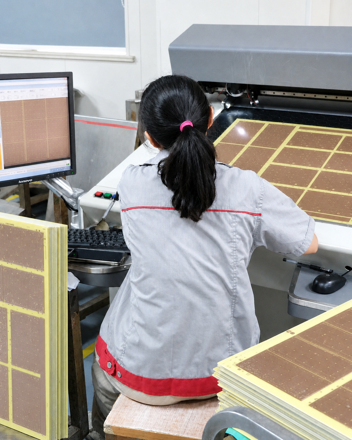
Every inner-layer copper image is optically inspected before lamination against the released image data. The program checks visible pattern conditions such as opens, shorts, residual copper and neckdowns before those layers are sealed into the build.

Post-Lamination Registration

Layer-to-layer registration is verified by the method defined for the construction and tooling route, including X-Ray where applicable. The evidence supports drilling and registration control but is not described as a guarantee that every internal condition has been detected.

100% Electrical Testing

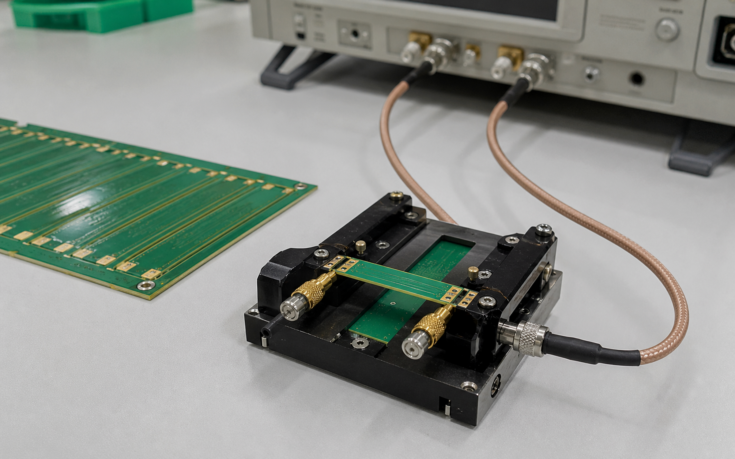
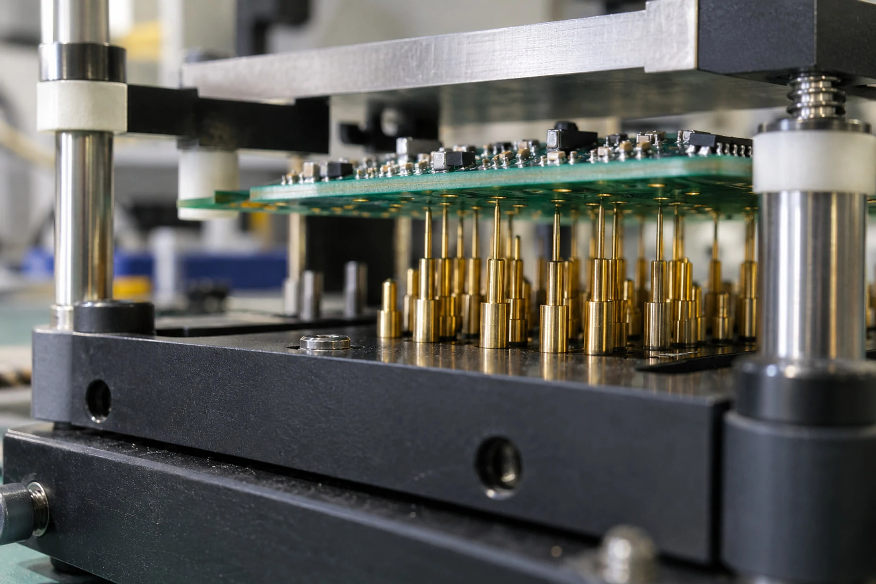
Every finished multilayer PCB receives 100% flying-probe or fixture-based continuity and isolation testing against the approved network data. The result confirms opens and shorts in the stated netlist; it does not replace material, plating, impedance or structural verification.

Microsection & Thermal-Stress Verification

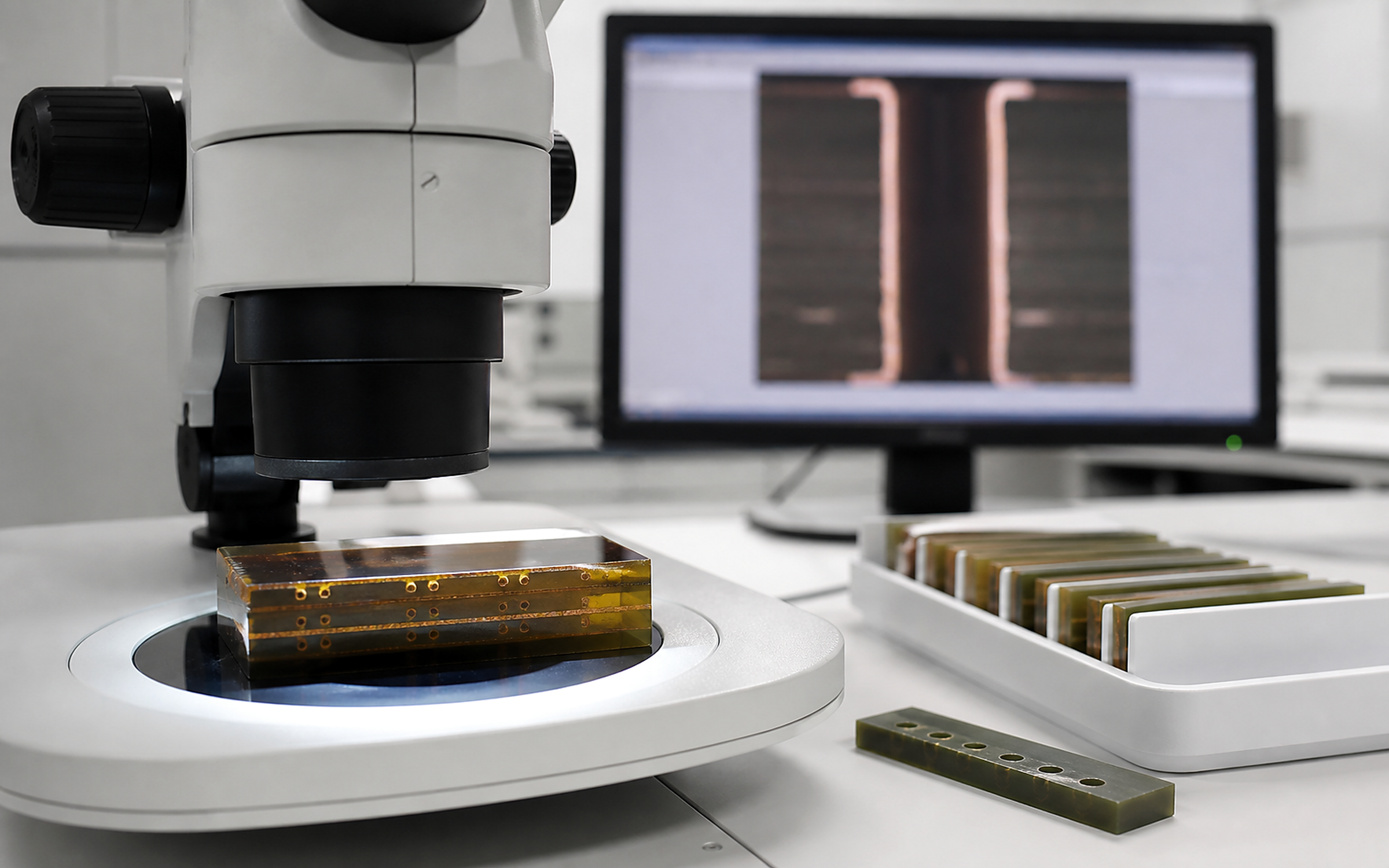
Production coupons or sampled specimens are examined at the lot, periodic or project frequency stated in the control plan. The applicable method may verify hole-wall copper, dielectric or registration characteristics and the selected structure after the defined thermal exposure.

Final Release Review

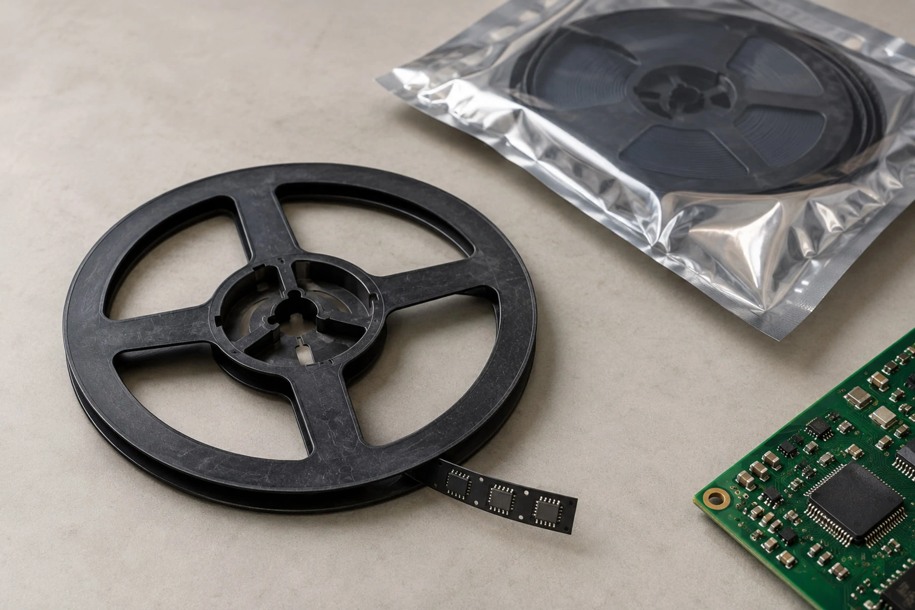
Finished boards are reviewed against the applicable visual, dimensional, solder-mask, marking and surface-finish requirements. IPC-A-600 supplies visual acceptance criteria, while performance class is defined through IPC-6012 and procurement documentation. Packaging is selected for the finish, storage period and shipping route.

Note: For advanced, high-tier inspection requirements (such as micro-sectioning analysis, localized environmental aging tests, etc.), please feel free to consult our technical team directly. We are fully equipped to support your customized engineering specifications.

Certifications &
Compliance

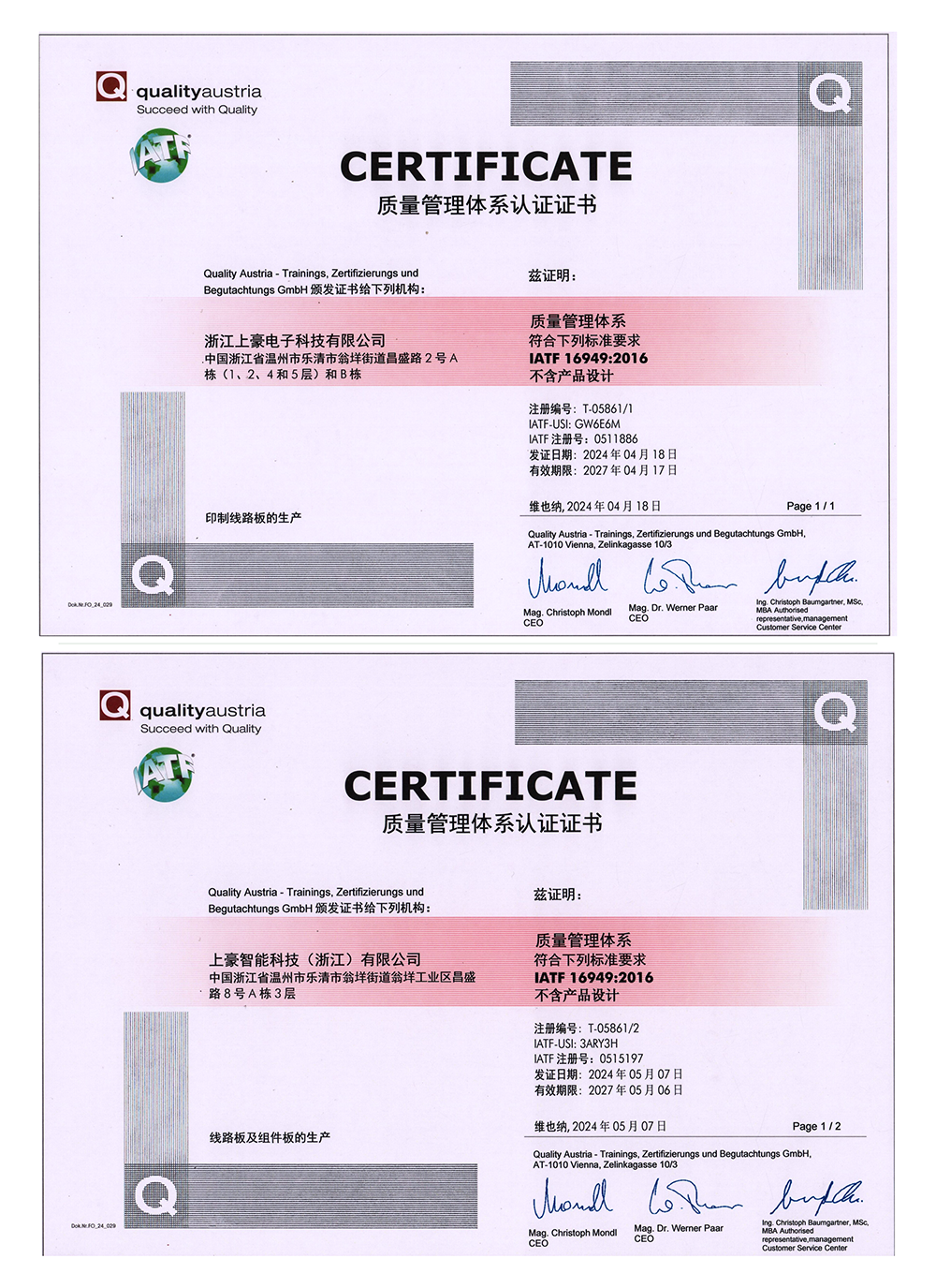
  • • IATF16949
  • • UL Certificate
  • • RoHS Compliance
  • • REACH Compliance
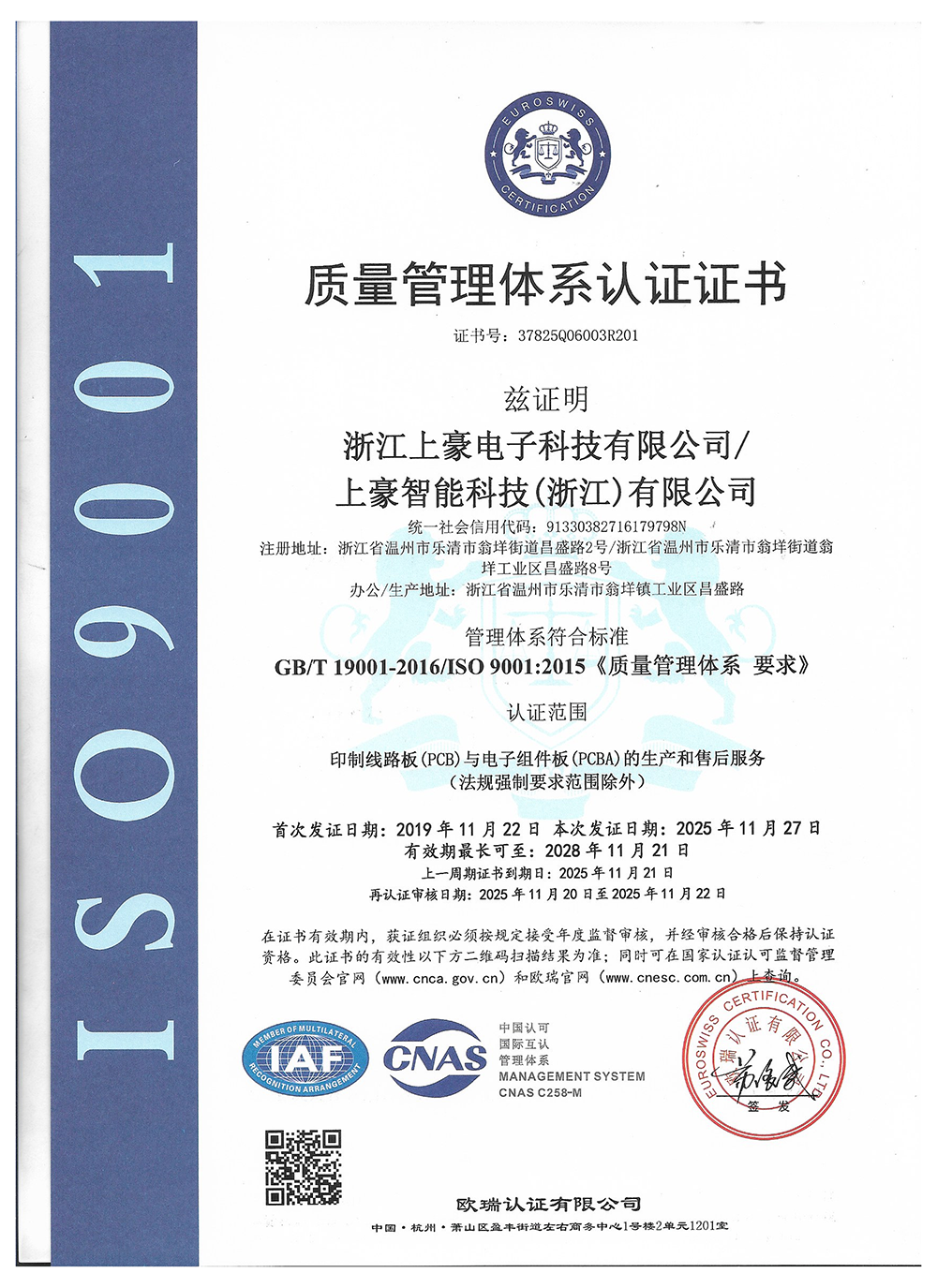
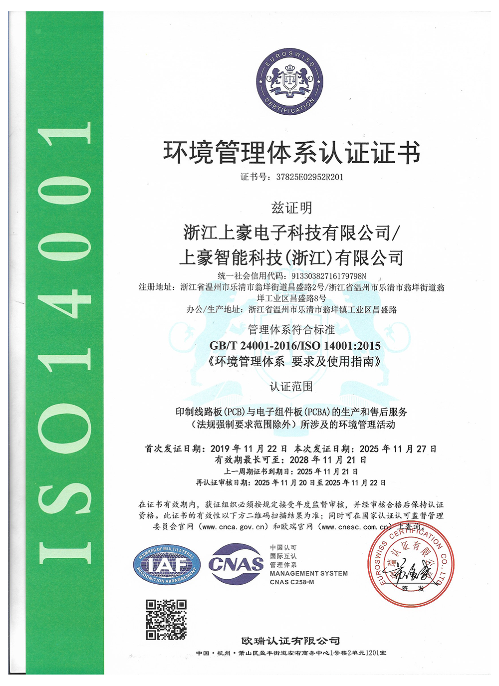
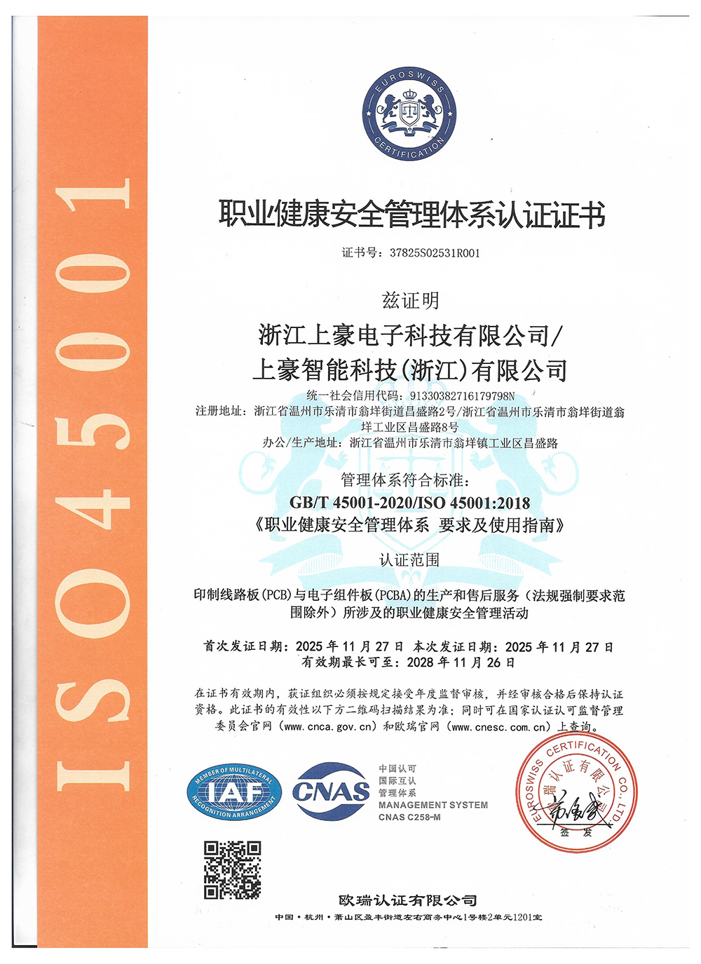
  • • ISO9001 / ISO14001 / ISO45001
More Certifications & Awards
IATF16949
IATF16949
ISO9001
ISO9001
ISO14001
ISO14001
ISO45001
ISO45001

Target Applications of Multilayer PCBs

Industrial Servo Drives & PLC Control Boards (Typically 4-6 Layers)

Integrates power distribution, motor drive signals, and control logic onto a unified board configuration. Dedicated internal power and ground planes help isolate electromagnetic noise, providing robust structural integrity against continuous operational heat and industrial vibration.

Product FAQ

Have more questions? 
Visit our Comprehensive FAQ Center for more detailed information.

View More FAQ

SUNHOPE’s published rigid-PCB range is 1–8 layers. By concentrating engineering, lamination, registration, drilling, plating and verification within this mature window, we support repeatable process control and cost-conscious production for industrial, consumer and other suitable electronics. PCBA assembly is available as a separate service for approved bare boards and assembly data; it is not described as a “1–8 layer PCBA capability.”