You're offline. Your information has been kept. Reconnect to continue.
We restored your unsaved quote details. Uploaded files still need to be attached again if this is a new browser session.
Thank you for contacting SUNHOPE. Our team will review your project information and aims to respond within 12-24 hours (GMT+8).
Your inquiry has been received. For complete quotation files or additional project data, you may also use Get a Quote.
PCB Manufacturing Services for1–8 Layer PCBs
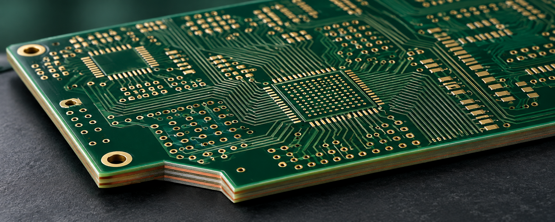
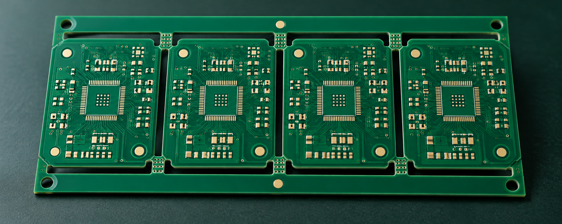
Every PCB begins as a set of electrical, mechanical and material decisions. SUNHOPE turns those decisions into manufacturable 1–8 layer rigid boards, supporting single-sided, double-sided and multilayer constructions together with controlled-impedance, high-Tg and high-frequency requirements. Before production, we review the released data, stack-up, materials and critical acceptance points so the manufacturing route remains aligned with the work the board has to perform.
Production Scope:Prototype Builds|Pilot Runs|Repeat Production
Since 1993Manufacturing Experience
15,000 m²Manufacturing Facility
300+Team Members
PCB and PCBA ScopeConnected Project Scope
Choose the Right PCB Manufacturing Route
Start with Construction Then Add the Technical Requirement
A useful PCB classification separates physical construction from technical requirement. First choose the layer structure that can carry the circuit. Then identify the material, signal or thermal controls the finished board requires. These two dimensions can be combined within the confirmed manufacturing range.
One conductive layer for straightforward circuits where cost discipline, repeatable production and efficient use of material matter. Suitable projects can use FR-4, paper-based, composite or aluminum-based constructions.
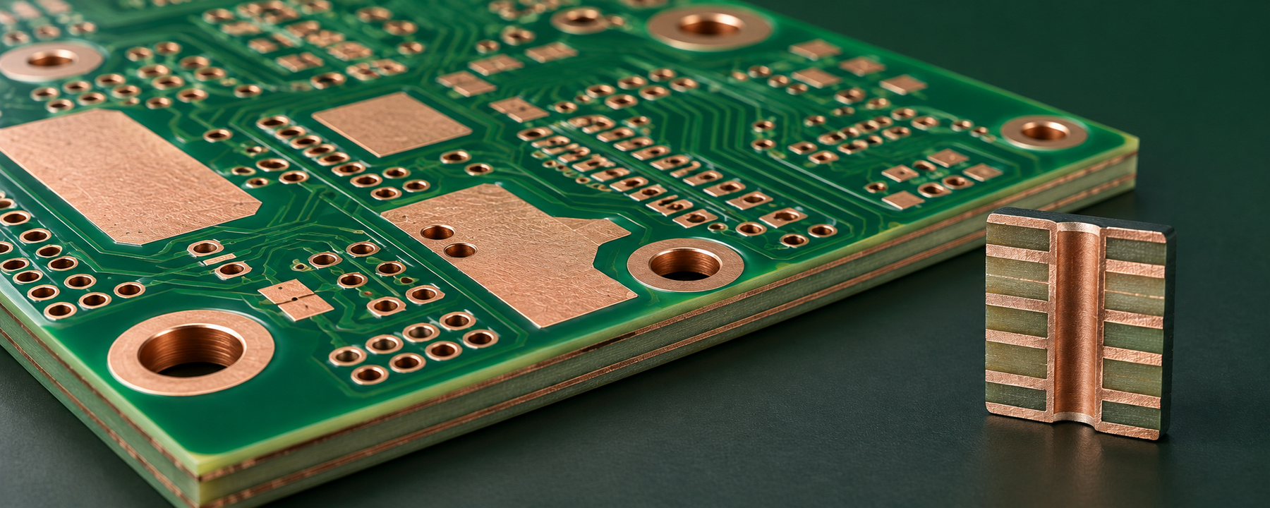
Two conductive layers connected through plated through holes provide more routing freedom, component-placement space and flexibility for power, ground and signal organization without moving directly to a multilayer structure.
Within SUNHOPE's 1–8 layer range, the multilayer offering focuses on 4–8 layer constructions that organize signal, power and ground relationships across a defined stack-up.
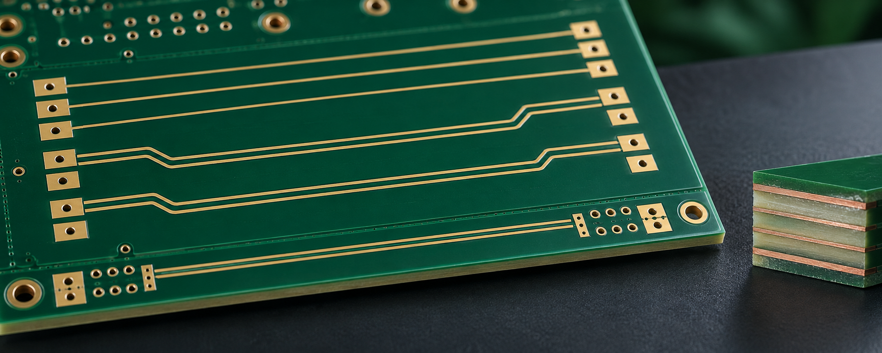
For transmission lines with an approved impedance target and tolerance. Stack-up, dielectric properties, copper thickness and conductor geometry are managed together, with TDR verification applied to the agreed coupon or test structure.
For assemblies or operating conditions that require more thermal-process margin from the laminate system. Tg is reviewed together with Td, Z-axis expansion, T260 or T288, moisture behaviour and the complete thermal profile.
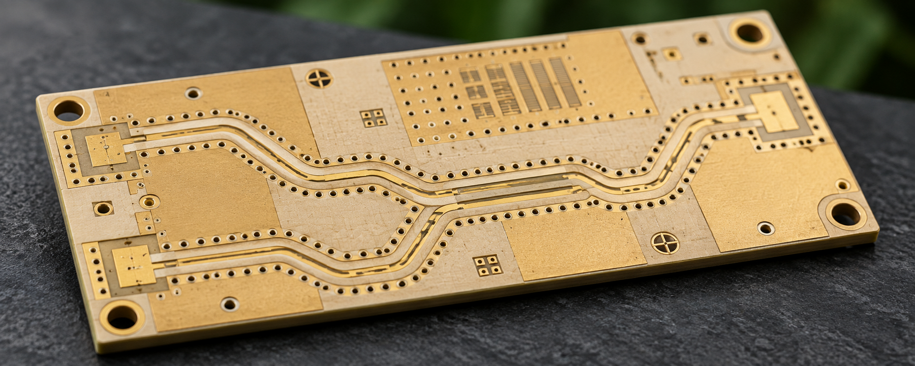
For RF and other high-frequency signal paths where Dk, Df, dielectric thickness, copper profile and conductor geometry influence loss, phase and impedance behaviour.
A PCB can belong to both groups. For example, a six-layer board may also require controlled impedance, a high-Tg material system or a selected high-frequency laminate. Final feasibility depends on the combined stack-up, material, geometry, finish, testing and acceptance requirements.
Manufacturing figures are useful only when their conditions are visible. The values below summarize SUNHOPE's current published PCB baseline. They provide an initial fit check and do not replace review of the complete design. Requirements near or beyond a published limit, or combinations of several demanding features, are evaluated before quotation and production release.
The Finish Is Matched To Assembly, Contact, Storage And End-Use Requirements
Match Requirements to Manufacturing Controls
What Changes When the Board Requirement Changes
Each requirement changes a different part of the manufacturing plan. Identifying that change early helps align the drawing, stack-up, material, process route and evidence before the board reaches production.
A Manufacturing Path Built Around theReleased Requirement
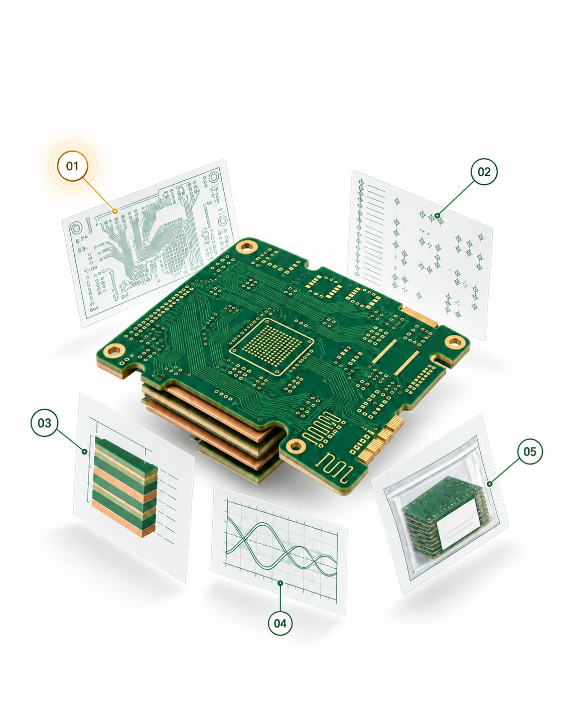
The route changes with the product, but the decision points remain connected. SUNHOPE uses the released design and agreed order requirements as the reference through engineering preparation, fabrication, verification and final delivery.
01Data and DFM Review
We review the applicable Gerber data, drill files, fabrication drawing, netlist and order requirements for completeness, consistency and manufacturability. Conflicting notes and features that may affect yield, cost or delivery are raised before release.
02Stack-up and Requirement Alignment
Layer sequence, material family, copper weight, finished thickness, surface finish, impedance targets and special acceptance needs are aligned with the proposed manufacturing route.
03CAM Preparation and Production Release
Manufacturing data, panelization, tooling and process instructions are prepared against the confirmed revision. An engineering query is returned when a manufacturing adjustment or unresolved conflict requires approval.
04Fabrication and Stage-Appropriate Control
The board proceeds through the applicable imaging, etching, drilling, plating, lamination, solder-mask, surface-finish and profiling operations. Checkpoints follow the construction and control plan rather than a single generic route.
05Verification Final Release and Packaging
Electrical, dimensional, structural, surface and project-specific checks are completed before release. Product identity, revision and batch linkage are confirmed, followed by protection suited to the board and shipment.
Quality Evidence and Traceability
Evidence Selected for theBoard Being Built
Quality control becomes more useful when each method answers a defined question. SUNHOPE combines circuit-image inspection, electrical testing, structural review and project-specific verification according to the product and approved control plan.
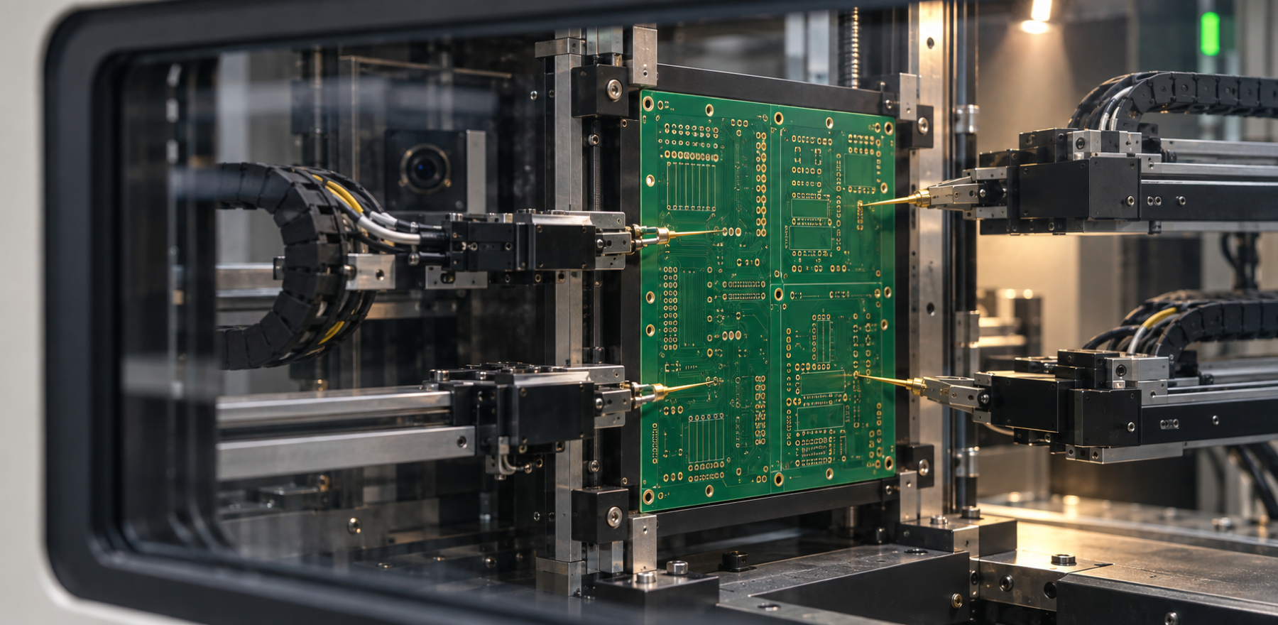
Circuit Pattern And Electrical IntegrityAOI is applied at the applicable circuit-image stage. Double-sided and multilayer boards receive 100 percent netlist testing by flying probe or a dedicated fixture to check continuity and isolation.
Geometry Surface And Assembly FitBoard outline, holes, thickness, routing or V-score, bow and twist, solder mask, legend and the applicable surface finish are reviewed against the approved requirement.
PTH And Multilayer StructureRegistration, X-ray, microsection or production-coupon analysis is applied where the board construction or control plan requires evidence of layer registration, plated-hole structure or dielectric construction.
Impedance And Signal PathControlled-impedance and related high-frequency boards use TDR measurement on the approved coupon or test structure. Report delivery follows the agreed project scope.
Material And Thermal RobustnessFor high-Tg and project-defined boards, material document review can be combined with specified thermal-stress, solderability or post-stress section analysis.
Release Traceability And ProtectionAvailable batch records connect product identity with applicable material, production, inspection and finished-product records. QR codes, barcodes or project-specific labels can be reviewed, followed by packaging selected for the product and shipment.
Why SUNHOPE for PCB Manufacturing
A Manufacturing Foundation You Can Examine
Since 1993, SUNHOPE has developed its PCB manufacturing scope inside a real production environment where engineering questions, process limits and customer requirements meet. Our value comes from keeping those elements connected throughout the project.
Single-sided, double-sided and 4–8 layer multilayer products share a defined rigid-PCB manufacturing range, with controlled-impedance, high-Tg and high-frequency requirements added by project.
Engineering before release
Material, stack-up, geometry, finish, marking, testing and acceptance requirements are reviewed together. Open points are clarified before they become assumptions in production.
Visible project communication
Released revisions remain connected with the agreed build. Engineering, material or process exceptions that may affect the requirement or schedule are communicated for decision.
A connected route into PCBA
Customers that need assembled boards can continue from in-house PCB manufacturing into SMT, THT or mixed assembly within one coordinated project path. Bare-board-only projects remain fully supported.
Project Fit and Industries
Built Around the Conditions the Board Will Meet
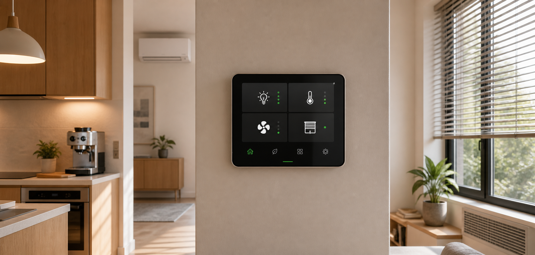
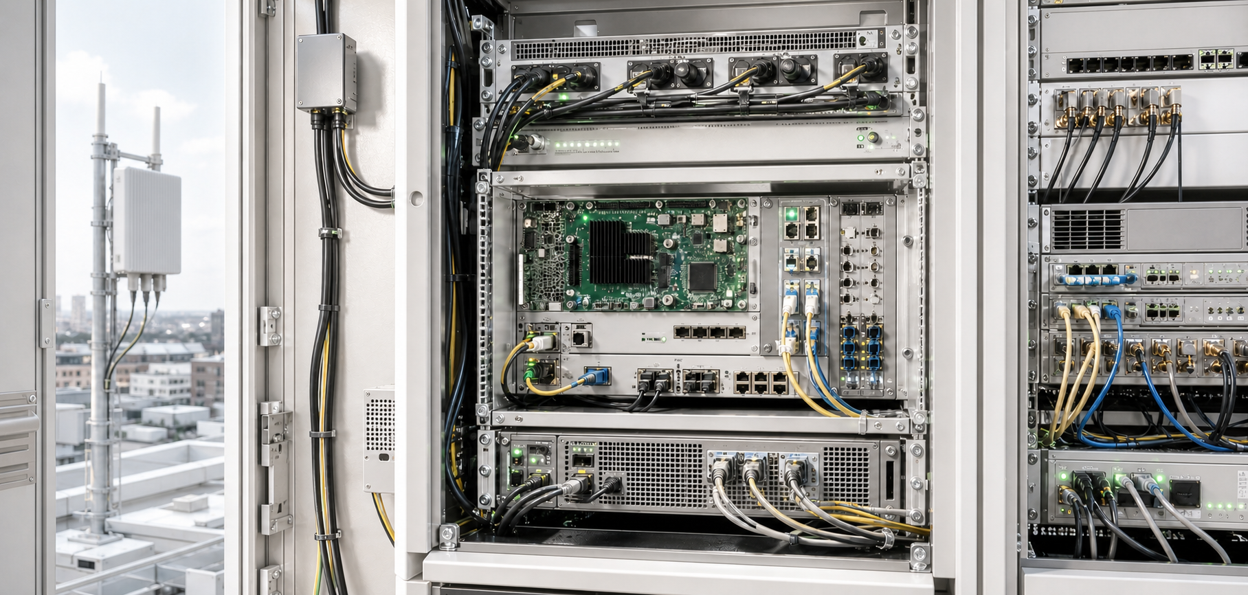
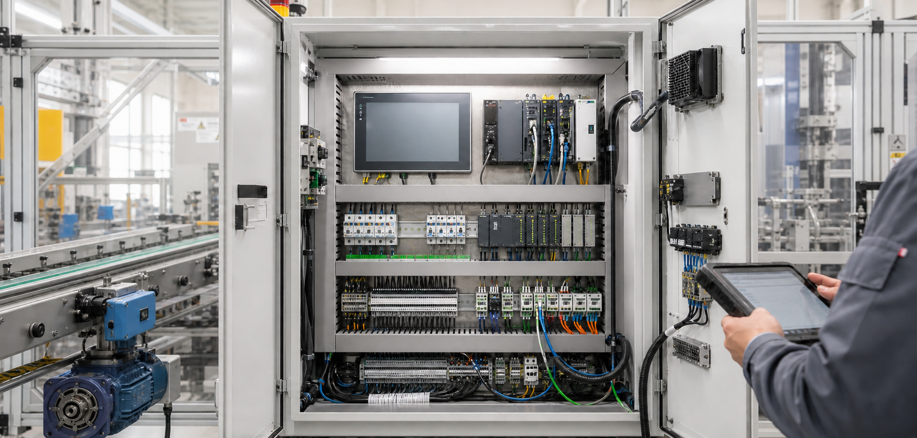
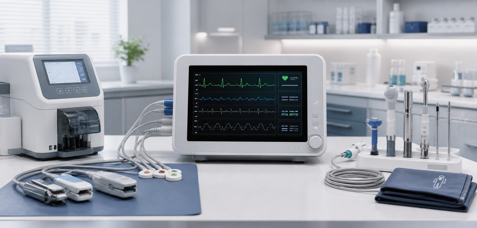
Industry context changes the questions a PCB manufacturer must ask. Product size, thermal exposure, signal behaviour, change authority, evidence and service-life expectations shape the manufacturing route before the first panel enters production.
Industry references describe manufacturing considerations and do not by themselves establish product certification or regulatory approval. Suitability is confirmed against the actual design, application and agreed requirements.
Select 01–05 to review each project input
01 · Manufacturing DataGerber manufacturing data · NC drill files · fabrication drawing · netlist where applicable
FILESFEASIBILITY REVIEWMANUFACTURING ROUTE
Prepare the Request and Start the Project
Prepare a Clear PCB Manufacturing Request
A useful quotation depends on more than board dimensions and quantity. Send the information available today, identify the items that are still open and state the requirements that must not change. Our team can then review feasibility, clarify missing decisions and prepare the manufacturing route around the released project scope.
Recommended PCB RFQ Information
Gerber manufacturing data and NC drill files
Fabrication drawing and netlist where applicable
Required quantity and whether the files represent a single board or an approved panel
Layer count, board dimensions, finished thickness and copper weights
Material family, Tg grade and stack-up requirements
Surface finish, solder-mask, legend and marking requirements
Impedance table, target values, tolerance and test-coupon information where applicable
Special holes, slots, routing, V-score, countersink, castellated or other mechanical features
Electrical, structural, material or report requirements and the applicable acceptance criteria
Packaging, labeling, destination and requested delivery schedule
SUNHOPE's published scope covers 1–8 layer PCBs, including single-sided, double-sided and multilayer constructions. Controlled-impedance, high-Tg and high-frequency requirements can be added within the confirmed project range.
Yes. Construction and technical requirement are separate dimensions. A multilayer board may also require controlled impedance, a high-Tg laminate, a high-frequency material or a combination of these requirements. The complete stack-up and process route must be reviewed together.
Yes. Applicable manufacturing data, drill files, fabrication drawing, netlist and order requirements are reviewed for completeness, consistency and manufacturability. Questions that affect tooling, process, inspection or delivery are clarified before production release.
SUNHOPE supports a published controlled-impedance tolerance of ±10%. TDR measurement is performed on the approved coupon or test structure, and reports are available upon request within the agreed project scope.
Yes. Customers may continue from SUNHOPE PCB manufacturing into SMT, THT or mixed assembly within one coordinated project path. Bare-board-only manufacturing is also supported.
The requirement is submitted for engineering review. Feasibility and any effect on material, tooling, process route, inspection, lead time or acceptance are clarified before the project is released.
No. A capability value describes a manufacturing baseline under defined conditions. Final feasibility depends on how layer count, board thickness, copper, hole structure, geometry, materials, finish, testing and acceptance requirements interact in the complete design.
Send the available Gerber data and NC drill files, together with the fabrication drawing, netlist where applicable, required quantity and delivery expectation. Include the layer count, finished thickness, copper weights, material, surface finish and any impedance, mechanical, testing or acceptance requirements. If some decisions remain open, identify them clearly so they can be reviewed before quotation and production release.
A clear build begins with a clear release.
Send the manufacturing data you have today. If the construction is already defined, we will review it against the current capability. If material, stack-up, impedance or acceptance points still need alignment, include those questions with the files.